

Why Does the 5V MCU Market Remain Strong?
2025-09-04 14:21:38 1764
Despite the growing prevalence of 3.3V in modern microcontrollers and the trend toward lower supply voltages in general system design, the 5V voltage level retains significant importance and remains a popular design approach. This is primarily because the higher 5V voltage offers superior noise immunity and signal transmission stability. Additionally, the physical characteristics of signal-to-noise ratio and the widespread use of 5V sensors ensure its continued relevance in high-interference environments like industrial control and automotive electronics. Moreover, selecting a 5V MCU does not necessitate compromising on modern MCU advantages like performance, low power consumption, or security. Several companies have launched new 5V MCUs, continuing to focus on industrial and reliability applications.
What are the advantages of 5V MCUs?
Interference Resistance
The 5V voltage offers stronger interference resistance than 3.3V, enabling superior performance in high-noise, high-interference application scenarios. For instance, industrial control and automotive electronics often require microcontrollers to operate stably in noisy environments. The 5V voltage better resists electromagnetic interference in such scenarios, ensuring stable and accurate signal transmission.
Signal Compatibility
Many traditional devices and peripheral components (such as older sensors and actuators) are designed based on 5V logic. When operating at 3.3V, microcontrollers often require level shifters to interface with these devices. Such conversion adds complexity to circuit design and may introduce delays or errors. Consequently, 5V microcontrollers remain the preferred choice for engineers working with 5V logic circuits.
How to determine the suitability of 3.3V versus 5V?
In practical design, how should one select the appropriate voltage level? This requires balancing specific application scenarios and design objectives. Below are some common considerations:
Low-power demand scenarios: Opt for 3.3V or even lower voltages
For devices with stringent low-power requirements—such as portable medical equipment, smart wearables, and remote monitoring devices—3.3V or lower voltages are more suitable. This significantly reduces power consumption, extends battery life, and alleviates thermal management pressures, offering advantages in miniaturized designs. Industrial Control and High-Interference Environments: Opt for 5V to Ensure Stability In industrial automation and high-interference settings, the 5V voltage level is typically prioritized. The higher voltage not only provides superior noise immunity but also minimizes signal attenuation and loss during transmission, ensuring data integrity. Furthermore, many industrial-grade sensors and actuators operate at 5V interfaces, making 5V microcontrollers more compatible. Cross-Platform and Communication Applications: Voltage Conversion and Adaptation In cross-platform or multi-device communication scenarios—such as IoT devices—mixed 3.3V and 5V systems may arise. This requires voltage adaptation via level-shifting chips. This design requires engineers to balance factors like power consumption, response speed, and signal integrity when selecting components to achieve effective communication between different voltage levels.
Texas Instruments MSPM0
Texas Instruments recently introduced the MSPM0H321x series MCUs, specifically engineered to address 5V system design challenges. These MCUs enhance system security, power efficiency, and performance while building upon the MSPM0 ecosystem. Suitable for applications including power tools, automotive systems, and kitchen appliances, this series facilitates seamless reuse of existing MSPM0-based code through pin-to-pin compatibility. Combined with the DriverLib API, it accelerates device replacement upgrades and simplifies software migration, integrating security, low power consumption, and high performance.
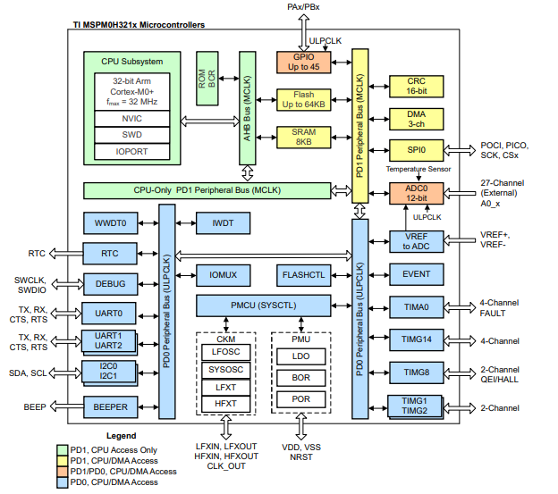
Figure. 1
Security: Building upon the MSPM0 platform's security foundation, it offers flexible and cost-effective security configuration capabilities. The Customer Security Code (CSC) hardware security architecture enables locking a custom root of trust, supporting secure boot with anti-rollback protection and secure firmware updates in the field to meet current and future security requirements.
Low Power: Despite the relatively higher power consumption of 5V MCUs, TI employs multiple techniques to reduce system power. The MSPM0H321x MCUs feature low-power performance and low-latency power mode transitions. This enables applications to “sleep as much as possible,” potentially saving additional power.
Using the MSPM0 System Control (SYSCTL) architecture, applications can achieve a low-power state of 3.5μA in standby mode while keeping SRAM, CPU, and peripherals in standby, and can resume operation within 20μs.
For scenarios requiring lower latency to receive commands via UART or I2C bus from standby, the MSPM0H321x series supports asynchronous fast clock requests. Such requests can trigger a fast clock when incoming data is detected, even before the CPU wakes up.
Features and Performance: While focused on low-power performance, the MSPM0H321x series combines analog and digital capabilities, powered by a 32MHz Arm® Cortex-M0+® CPU with single-cycle multiplication extension, up to 64kB of flash memory, and 8kB of SRAM. The 12-bit ADC operates at sampling rates up to 1.5MSPS with up to 27 input channels, supporting a wide range of control and sensing applications.
The advanced control timer (TIMA) features enhanced PWM generation modes for complementary pairs with dead-time functionality and ultra-low-latency fault handling. Additionally, the MSPM0H321x series offers multiple package options, including two with 0.8mm pin pitch for ultra-low-cost PCB assembly processes. Since the MCU's introduction, embedded engineers have continually sought innovative ways to leverage these versatile devices.
The MSPM0 product family includes devices supporting supply voltages from 1.62V to 3.6V, enabling engineers to adopt lower operating voltages, thereby reducing system power consumption and lowering cost requirements. However, modern MCUs supporting 5V supply voltages remain essential.
In applications featuring traditional 5V circuitry or complex noise immunity challenges, the MSPM0H321x MCU enables hardware designers to operate natively within 5V systems while benefiting from innovative security, low-power, and performance features.
NXP MCX E
As edge applications operate in increasingly harsh environments, demands for microcontroller resilience continue to rise. The MCX E series, based on the Arm Cortex-M4F core, was developed specifically for stable control in scenarios with extremely complex electrical and thermal environments.
The MCX E24, the first product in this series, delivers the performance, security, and reliability required for industrial automation, smart home appliances, and energy control. It not only serves current edge applications but also provides a solid foundation for future expansion.
As edge device deployments expand, designers must account for increasingly demanding application environments. Developers face mounting challenges: - Electromagnetic interference (EMI) may compromise system stability - Extreme temperatures and 24/7 operation demand higher component tolerance - More connected devices broaden potential attack surfaces and elevate security risks Integrating functional safety, cybersecurity, and high performance within resource-constrained edge devices increases development complexity. NXP deeply understands the evolving technical demands of edge computing. The MCX E-series is engineered to address these challenges. It combines robust 5V power supply support, industrial-grade temperature tolerance, built-in security diagnostics, and secure configuration options. This enables developers to build reliable and secure systems without compromising performance.
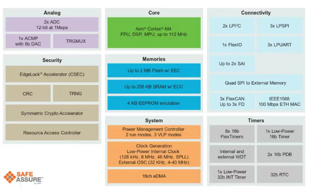
Figure. 2
The MCX E24 integrates enhanced noise immunity and high-precision mixed-signal processing, making it suitable for industrial automation, smart home appliances, and other fields while laying the foundation for future expansion. Equipped with an 112MHz Arm Cortex-M4 processor supporting floating-point operations and DSP extensions, along with corresponding memory and multiple modules, it meets the demands of high-response-deterministic closed-loop applications. Combined with relevant software libraries, it enables efficient implementation of advanced control algorithms.
For durability and safety assurance, the MCX E24 supports a 2.7V to 5.5V voltage range and operates within -40°C to 125°C, meeting 10-year lifecycle standards. It features a comprehensive functional safety architecture supporting up to SIL 2 compliance under IEC 61508, along with multiple hardware diagnostics and supporting documentation. Integrated data security mechanisms support secure programming and encryption, ensuring end-to-end lifecycle protection.
Furthermore, the MCX E series leverages the MCUXpresso Developer Experience ecosystem, supporting multiple IDEs and flexible toolchains to accommodate diverse development styles, empowering developers.
Renesas RX660
Several years ago, Renesas announced the RX660 series microcontrollers (MCUs) as a new addition to its RX 32-bit MCU family. This series supports operating voltages up to 5V, delivering exceptional noise immunity for home appliances and industrial equipment exposed to high electromagnetic interference. The RX660 is the first device in Renesas' high-end RX general-purpose MCU lineup to support 5V voltage and the first in the RX series to integrate a CAN FD controller for high-speed data communication. The new RX660 MCU's high operating voltage eliminates the need for additional noise suppression components often required by current 3V MCUs. This helps customers reduce development time, lower component costs, and enhance system quality.
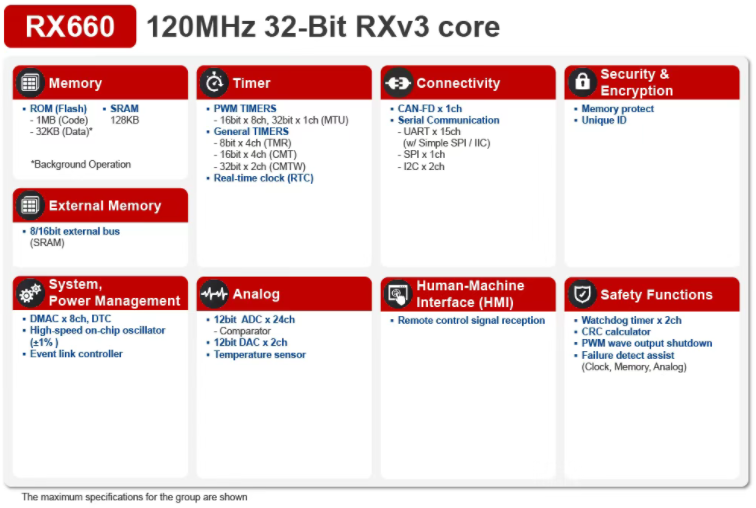
Figure. 3
In recent years, as functional safety and cybersecurity have become critical components of electronic systems, software scale has expanded accordingly. With increasing product variants, more devices incorporate real-time operating systems to simplify software maintenance. Additionally, product designs must accommodate future feature enhancements delivered via wireless (OTA) updates. To address these demands, Renesas has developed the RX660. This device utilizes the RXv3 core (6.00 CoreMark/MHz) and operates at up to 120 MHz, delivering high performance and outstanding energy efficiency. It features a large ROM capacity of up to 1 MB and RAM of up to 128 KB, with multiple package options ranging from 48 to 144 pins. Notably, the number of effective pins for general-purpose I/O is 10% higher than the earlier RX210, while maintaining 5V voltage compatibility. For example, the 144-pin version of the RX660 offers 134 effective pins, 11 more than the RX210. With increased I/O count, MCUs in the same package can connect more sensors, simplifying upgrades to existing systems.
“Noise suppression is critical for home appliances and industrial products, as electromagnetic waves in the surrounding environment can cause system failures or performance degradation,” said Sakae Ito, Vice President of Renesas' IoT Platform Business Unit. "We introduced the new RX660 MCU to meet strong customer demand for high power supply voltage designs. We are pleased to assist customers in streamlining their product design processes."
CAN is gaining widespread adoption in industrial equipment and robotics. However, the increasing use of numerous sensors leads to rising data communication volumes, causing bandwidth shortages and higher costs due to the need for multiple buses. The RX660 is the first in the RX series to integrate a CAN FD controller, enabling fast, high-capacity data transmission. CAN FD enables transmission of multiple safety signals within a single frame, thereby enhancing equipment safety.
GigaDevice GD32C231
GigaDevice has also recently announced the official launch of its value-driven GD32C231 series entry-level microcontrollers, further expanding its product lineup based on the Arm Cortex-M23 core. As a leader in China's Arm MCU market, GigaDevice positions the GD32C231 series as a “high-performance entry-level” solution. It will deliver more competitive options for applications including small appliances, BMS battery management systems, small-screen display devices, handheld consumer products, industrial auxiliary control, and automotive aftermarket systems. Leveraging cumulative shipments exceeding 2 billion MCUs and a mature supply chain system, GigaDevice's GD32C231 series breaks performance limitations typical of entry-level chips through innovative design. This series not only integrates rich peripherals but also adopts industrial-grade wide-voltage process technology and a comprehensive ecosystem. While maintaining exceptional cost-performance, this affordable MCU can handle more complex application scenarios, redefining the value standards of the entry-level MCU market and pioneering a new paradigm of “affordable without compromising specs.”
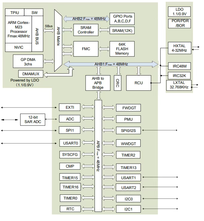
Figure. 4
GD32C231 Series MCUs: The Ultimate Choice for Cost-Performance Ratio The GD32C231 series MCUs deliver a significant upgrade in cost-performance ratio by substantially enhancing computational performance and peripheral specifications while maintaining outstanding price competitiveness. This series adopts Arm's advanced Cortex-M23 core architecture, delivering 10% higher performance than Cortex-M0+ with a clock speed up to 48MHz. It features efficient processing capabilities such as single-cycle multiplication and integer division, substantially improving software execution efficiency. For memory configuration, it incorporates 32KB to 64KB of highly reliable embedded Flash and 12KB of low-power SRAM, with ECC error correction enabled across the entire memory area. To accommodate diverse application requirements, multiple packaging options are available: TSSOP20/LGA20, QFN28, LQFP32/QFN32, and LQFP48/QFN48. The highly integrated chip design effectively reduces the number of external components, providing users with a more cost-effective Bill of Materials (BOM) solution.
GD32C231 Product Family: Perfect Balance of Wide Voltage Range, Low Power Consumption, and Fast Wake-up The GD32C231 offers outstanding power flexibility and low power consumption, supporting a wide voltage supply range of 1.8V to 5.5V and a wide operating temperature range of -40°C to 105°C, making it suitable for various harsh environments. The chip offers multiple power management modes, achieving sub-5μA current consumption in deep sleep while maintaining rapid responsiveness with a 2.6μs wake-up time. This perfectly balances low power consumption with real-time requirements, empowering battery-powered and portable device applications.
The GD32C231 also excels in security and reliability: Exceptional electrostatic discharge (ESD) protection meets stringent standards of 8KV contact discharge (CD) and 15KV air discharge (AD); Full Flash/SRAM incorporates ECC error correction design to effectively prevent data corruption; integrated hardware CRC modules ensure data transmission integrity and reliability. These features enable stable operation in safety-critical domains like industrial control and automotive electronics.
Highly Integrated Peripheral Resources Empower Diverse Application Scenarios The GD32C231 integrates rich peripheral resources, significantly enhancing system integration and application flexibility: - Built-in 12-bit ADC (supporting 13 external channels) and 2 internal comparators meet precision measurement needs; - Provides up to 4 general-purpose 16-bit timers and 1 16-bit advanced timer. It incorporates 2 high-speed SPI interfaces (supporting 4-wire QSPI mode at up to 24Mbps), 2 I2C interfaces (supporting Fast Mode+ at 1Mbit/s), and 3 UARTs (6Mbps), along with 3 DMA controllers and 1 I2S controller, ensuring efficient communication capabilities. It also delivers outstanding GPIO expandability, supporting up to 45 GPIO pins in a 48-pin package, significantly enhancing hardware design flexibility. These specialized configurations enable the chip to effortlessly handle diverse application scenarios such as industrial control and consumer electronics.
Summary
Beyond the above, many MCU manufacturers are continuously advancing the development of 5V MCUs, introducing new innovations. After all, MCUs have extensive applications, and power consumption is not the sole parameter. Leading MCU manufacturers including Infineon, Microchip, ST, and others have extensively deployed 5V products to meet the demands of MCUs in harsh environments like industrial settings.
The distinction between 3.3V and 5V voltage levels reflects not only the adaptability needs of microcontrollers across different application scenarios but also represents a balance between power management and anti-interference performance. In portable devices or other low-power applications, 3.3V is gradually becoming the mainstream choice. However, in industrial control and high-interference environments, 5V continues to hold irreplaceable advantages.


