

EP2C5T144C8N FPGAs: Features, Applications and Datasheet
2025-11-13 10:32:09 1665
EP2C5T144C8N Description
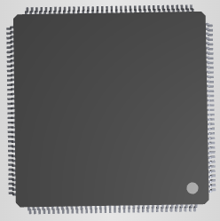
The EP2C5T144C8N is a member of the Altera Cyclone II FPGA family, designed to deliver high performance at low cost. Built using a 90 nm CMOS process, this FPGA offers a balance of logic density, low power consumption, and rich I/O options. It is housed in a 144-pin TQFP package, making it ideal for cost-sensitive and space-constrained applications such as embedded systems, communications, and consumer electronics.
EP2C5T144C8N Features
Logic Elements (LEs): 4,608
Embedded Memory: 119,808 bits of RAM
Embedded Multipliers: 26 × 18×18-bit multipliers
Phase-Locked Loops (PLLs): 2 PLLs for clock management
I/O Pins: 89 user I/O pins
Configuration Options: Supports Active Serial (AS), Passive Serial (PS), and JTAG modes
Operating Speed Grade: –8 (C8N indicates commercial temperature range)
Package Type: 144-pin TQFP
Low Power Consumption: Designed for efficient power use in portable or thermally constrained designs
EP2C5T144C8N Applications
Industrial control systems
Embedded computing platforms
Communications and networking equipment
Consumer electronics
Educational and research FPGA development boards
Motor control and signal processing systems
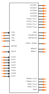
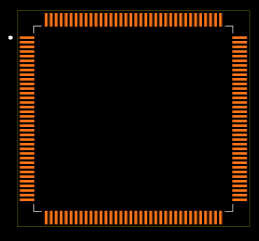
EP2C5T144C8N CAD Model
Symbol
Footprint
3D Model

EP2C5T144C8N Alternatives
EP2C5T144I8N – Industrial-grade variant of the same device
EP2C8Q208C8N – Higher logic density alternative within the Cyclone II family
EP3C5E144C8N – Newer generation (Cyclone III) with lower power and improved performance
XC3S500E-4TQG144C (Xilinx Spartan-3E) – Cross-vendor equivalent FPGA
Lattice LCMXO2-1200HC-4TG100C – Low-power CPLD alternative for smaller designs
EP2C5T144C8N Manufacturer
Intel Corporation is a global leader in semiconductor innovation, headquartered in Santa Clara, California, USA. Founded in 1968 by Robert Noyce and Gordon Moore, Intel is best known for inventing the world’s first commercial microprocessor and driving the evolution of modern computing.
Intel designs and manufactures a wide range of products, including microprocessors, chipsets, memory, FPGAs, AI accelerators, and networking solutions. Its technologies power everything from personal computers and data centers to cloud infrastructure, autonomous vehicles, and IoT devices.
Through continuous innovation in advanced process technology, architecture design, and AI-driven computing, Intel remains at the forefront of the semiconductor industry — enabling the world’s digital transformation and shaping the future of intelligent computing.
EP2C5T144C8N FAQs
What configuration methods are supported by the EP2C5T144C8N?
It supports Active Serial (AS), Passive Serial (PS), and JTAG configuration modes, allowing flexibility for both standalone and system-based designs.
What is the maximum user clock frequency supported by the device?
The EP2C5T144C8N can typically handle core clock frequencies up to 250 MHz, depending on design complexity and routing constraints.
How much on-chip memory does the EP2C5T144C8N provide?
It integrates 119,808 bits (approximately 14.6 KB) of embedded dual-port RAM, ideal for buffering, caching, or small data storage.
Is the EP2C5T144C8N pin-compatible with other Cyclone II devices?
Yes, it is pin-compatible with other devices in the same package (TQFP-144) within the Cyclone II family, allowing easy scalability in design upgrades.
What voltage levels are supported for I/O banks?
The I/O banks support multiple standards including 3.3V LVTTL, 2.5V, and 1.8V LVCMOS, offering flexibility for mixed-voltage system interfaces.


