

GAA+PVT Dual-Drive: Semiconductor Technology Breakthroughs and Chip Efficiency Revolution
2025-10-09 11:02:04 758
As process technologies continue to evolve, design tools and the IP they rely on must keep pace. One example of industry progression is seen in Process-Voltage-Temperature (PVT) monitoring IP. Embedded within chips, PVT monitors provide feedback on silicon health throughout every stage of the lifecycle. Data collected from these monitors delivers numerous benefits, such as early prediction of impending chip failures and tracking trends across “massive” deployments of chips worldwide.
From FinFET to GAA
FinFETs first appeared at the 22nm process node. Their fin-like structure is surrounded on three sides by the gate, enabling superior channel control. However, as process technology advances toward 5nm and 3nm nodes, transistor sizes approach the physical limits of atomic dimensions. Improving chip performance, power efficiency, area cost, and time-to-market simultaneously through traditional 2D scaling under Moore's Law becomes increasingly challenging. FinFET transistors also face growing challenges in driving current, electrostatic control, and leakage issues.
For instance, as FinFETs scale down, the fins forming the transistor gate become taller and narrower. This makes them more fragile and prone to bending during manufacturing, thereby degrading performance and power efficiency. Simultaneously, statistical data indicates that each new process shrink reduces the contact area per transistor node by approximately 25%. Smaller area leads to higher resistance, with interface resistance between metal contacts and silicon transistors, along with external resistance within the source and drain regions, being the primary contributing factors.
Consequently, the industry is rapidly shifting toward Gate-All-Around (GAA) transistors. This innovative structure allows the gate to surround the channel from all sides, enabling continued process scaling.
Early GAA devices employed vertically stacked nanosheet structures. These nanosheets consist of independent horizontal layers, each encapsulated by gate material. In FinFET transistors, achieving higher current requires arranging multiple fin structures side-by-side; GAA transistors, however, can enhance current carrying capacity by vertically stacking just a few nanosheets. This dimensional flexibility allows transistors to meet specific performance requirements.
Channel control represents another significant difference between FinFET and GAA transistors. Compared to FinFET transistors, GAA transistors offer superior channel control. The gate's full-perimeter encapsulation of the channel effectively suppresses short-channel effects while reducing leakage from the device's untouched bottom. As process nodes continue to shrink, nanolayer dimensions will evolve, potentially approaching nanowire configurations.
Moreover, the method for controlling fin width in GAA transistors shifts from lithography and etching to epitaxy and selective removal, enabling greater precision. From a performance perspective, the GAA architecture reduces variability while supporting gate length scaling, increasing drive current by 10% to 15% while simultaneously lowering power consumption.
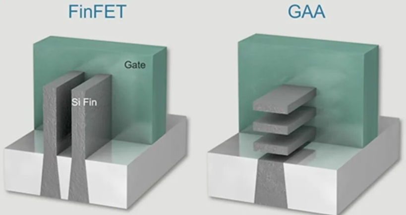
Figure. 1 FinFET vs. GAA Transistor Structure Comparison (Source: Applied Materials)
Real-Time PVT Monitoring in Silicon Lifecycle Management
As previously discussed, amid increasingly complex chip architectures, continuous process node scaling, and ever-demanding application requirements, new approaches—including novel system architectures, 3D transistor structures, advanced materials, and packaging technologies—are being explored to achieve logic scaling goals. However, this approach also introduces multiple challenges, such as spatial process variations, thermal hotspots, voltage droops, and unpredictable application loads, rendering traditional static margining methods inadequate.
Within this context, Silicon Lifecycle Management (SLM) has emerged as a foundational strategy for optimizing the performance, reliability, and energy efficiency of semiconductor devices throughout their entire lifecycle. At the core of effective SLM lies the Process-Voltage-Temperature (PVT) monitor—a silicon-verified, high-precision sensor embedded within the chip that provides real-time visibility into the device's operational state based on its intrinsic silicon characteristics.
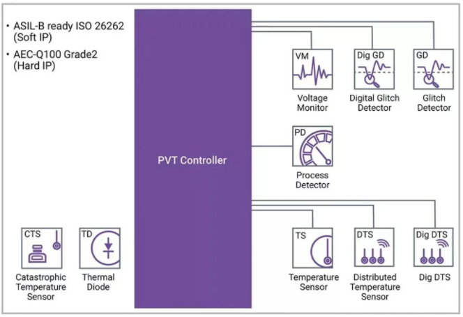
Figure. 2 PVT Controller (with PVT Monitor IP Core)
Simply put, the four pillars of SLM are Monitor, Transport, Analyze, and Act. By establishing a continuous “state visibility-active execution” loop, it achieves optimization across the entire lifecycle of modern chips.
For instance, during the chip design phase, embedded monitors collect critical data such as process variations, voltage fluctuations, and thermal behavior. This data is then transmitted to a centralized SLM database for analysis at the chip, edge, or cloud level. During the design phase, engineers can refine chip designs based on real-world feedback from test silicon. In the operational deployment phase, the system initiates real-time automated responses to achieve performance tuning, power reduction, and extended device reliability and lifespan.
How to Better Support GAA
From a circuit design perspective, GAA transistors are highly suited for digital circuits—welcome news for digital designers. GAA transistors offer superior channel control and scalability, enabling the design of efficient logic gates and memory cells. Adopting GAA technology allows digital circuits to achieve performance gains and reduced power consumption, fully leveraging its benefits.
However, the benefits for analog circuit designers are less clear-cut. Achieving the same level of precision in analog circuits as in digital circuits may present significant challenges. Analog designers must explore new technical approaches to fully leverage the advantages of fully-surrounding gate transistors. For instance, the use of bipolar devices like bipolar junction transistors (BJTs), currently prevalent in mixed-signal applications, may gradually decline.
Therefore, to maintain leadership and adapt to the emergence of GAA transistors, PVT monitor IP design must undergo significant innovation. Currently, the lack of characterization for bipolar junction transistors and thick-oxide field-effect transistors (FETs) is a key driver for such design innovation, propelling sensing technology toward digital solutions. Simply put, adapt and evolve, or risk rapid obsolescence.
Digital technology offers not only the additional advantage of reduced area/footprint but also eliminates the need for analog signal protection against noise/crosstalk. As technology transitions to digital, measures like analog line shielding become unnecessary.
System-on-Chip (SoC) and IP suppliers must find innovative ways to maintain accuracy comparable to analog circuits—a capability that will become a key differentiator.
This shift toward digital sensing offers significant industry benefits: reduced power consumption, increased conversion rates, and simplified implementation of PVT monitoring IP. It enables flexible deployment of more remote sensors closer to target sensing points. For temperature sensors, placing sensors near heat sources minimizes temperature gradient effects. Multiple sensors also enhance accuracy through triangulation. This represents a win-win scenario across all dimensions.
Synopsys' Comprehensive PVT IP Subsystem
Synopsys' PVT IP subsystem comprises a full suite of monitors, a dedicated central controller, and supporting infrastructure. Core components include Process Detectors (PD), Voltage Monitors (VM), and Glitch Detectors (GD, Digital GD). For thermal monitoring, the subsystem incorporates various sensors such as Temperature Sensors (TS), Distributed Temperature Sensors (DTS and Digital DTS), Catastrophic Temperature Sensors (CTS), and Thermal Diodes (TD). Among these, only Thermal Diodes and CTS operate asynchronously. The remaining sensors are managed by a central PVT controller with software drivers and interconnected via a dedicated software serial bus.
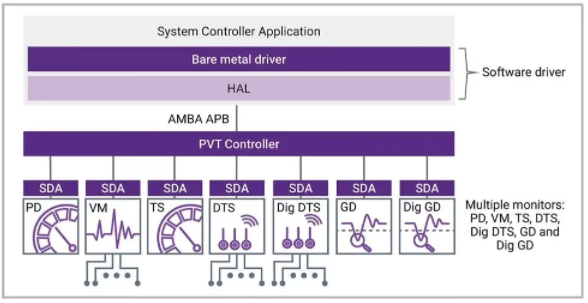
Figure. 3 Reference Bare-Metal Software Driver
Crucially, all PVT IP has been validated across multiple foundries and process nodes, ensuring future-proof compatibility. Currently supported nodes include TSMC's N6, N5A, N4P, N3E/P, N3A, and N2P; nodes under development include Intel Foundry Services (IFS) 18A and Samsung SF4X. As the IP portfolio continues to expand, new offerings like the digital DTS1 and digital glitch detector further enhance digital compatibility while reducing integration costs.
Additionally, Synopsys' PVT IP solutions are tailored for automotive-grade applications where reliability and safety are paramount. Hard IP has passed AEC-Q100 Grade 2 testing, while soft IP components comply with the ISO 26262 functional safety standard, meeting ASIL B requirements.
Let's examine application examples of PVT IP solutions in several typical scenarios:
1. Artificial Intelligence (AI) Processors
In AI system-on-chip (SoC) designs, high computational density and burst-based workloads exacerbate thermal management and power consumption challenges. PVT monitors enable low-latency thermal management, dynamic IR drop control, and optimized power margin allocation for critical logic. These capabilities ultimately enhance core utilization, boost performance per watt, and reduce operational costs.
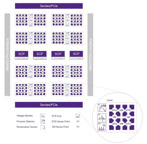
Figure. 4 Practical Application of PVT IP Solutions in AI Processors
2. Data Centers and High-Performance Computing (HPC)
Reliability and energy efficiency are paramount in cloud environments and HPC scenarios. Embedded PVT monitors support real-time power optimization, multi-core thermal analysis, and reliability prediction, enabling data centers to scale steadily while reducing CO₂ emissions and lowering total cost of ownership (TCO).
3. 5G and Consumer Devices
For 5G smartphones and consumer electronics, PVT monitors address thermal management challenges and enhance battery efficiency. Supporting core voltage regulation, real-time thermal management, and performance tuning, they optimize user experiences during video streaming, gaming, and multitasking while extending device runtime and improving responsiveness.
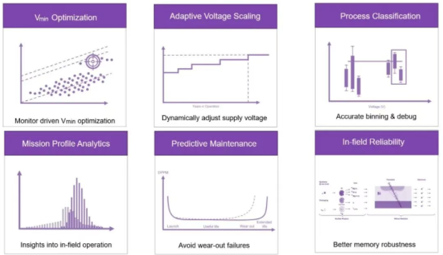
Figure. 5 Target Application Areas for SLM IP
Conclusion
The GAA transistor revolution has commenced, poised to overcome FinFET limitations and propel Moore's Law forward. Industry observers widely agree that advancing along this technology path is inevitable for all chip, IP, SoC developers, and foundries. Manufacturing processes and equipment will evolve accordingly, particularly as the industry adopts true 3D devices. All chip designers should prepare to embrace a new era in semiconductor technology.


