

XC6SLX9-2FTG256C FPGAs: Features, Applications and Datasheet
2025-10-10 15:36:39 1194
XC6SLX9-2FTG256C Description
The XC6SLX9-2FTG256C is a member of the Xilinx Spartan-6 FPGA family, designed for cost-sensitive applications requiring optimized performance, low power consumption, and a rich logic feature set. It is built on a 45 nm low-power process technology, offering a balance between logic density, DSP performance, and embedded memory resources. This FPGA provides high-speed connectivity, flexible configuration options, and efficient power management, making it ideal for a broad range of embedded and communication systems.
XC6SLX9-2FTG256C Features
Logic Resources: 9,152 logic cells and 9152 flip-flops for flexible digital design implementation.
Memory: Includes 576 Kbits of block RAM with integrated error correction support.
DSP Performance: 16 DSP slices optimized for arithmetic and signal-processing tasks.
I/O Flexibility: Up to 186 user I/O pins in the FTG256 package, supporting LVDS, LVCMOS, and SSTL standards.
Clock Management: Dual digital clock managers (DCMs) and PLLs for precise clock generation and jitter reduction.
Low Power Operation: Dynamic power scaling with multiple voltage options (core voltage at 1.2 V).
Configuration Options: Supports SPI, JTAG, and slave-serial configuration modes.
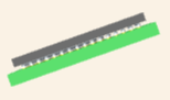
Packaging: Compact FTG256 BGA package suitable for high-density PCB layouts.
XC6SLX9-2FTG256C Applications
Embedded Control Systems: Custom logic, peripheral interfacing, and data processing.
Communication Equipment: Protocol bridging, packet processing, and SERDES-based connectivity.
Consumer Electronics: Image processing, video control, and sensor data fusion.
Industrial Automation: Real-time control, signal conditioning, and programmable I/O expansion.
Education and Research: FPGA-based prototyping, hardware training, and algorithm acceleration.
XC6SLX9-2FTG256C CAD Model
Symbol
Footprint
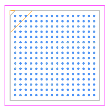
3D Model

XC6SLX9-2FTG256C Alternatives
Lattice LCMXO3LF-6900C – Lower power, smaller footprint FPGA for simpler logic designs.
Intel (Altera) Cyclone IV EP4CE10F17C8N – Similar density and speed with strong DSP support.
Xilinx Artix-7 XC7A15T-1FTG256C – Higher performance successor with more advanced transceivers.
Gowin GW2A-18 – Compact FPGA option with embedded memory and lower cost for control applications.
XC6SLX9-2FTG256C Manufacturer
Advanced Micro Devices, Inc. (AMD) is a global leader in high-performance computing, graphics, and semiconductor technologies. Founded in 1969 and headquartered in Santa Clara, California, AMD designs and develops a broad range of products including central processing units (CPUs), graphics processing units (GPUs), field-programmable gate arrays (FPGAs), and adaptive SoCs (System-on-Chip) solutions.
AMD is best known for its Ryzen™ processors, Radeon™ graphics cards, and EPYC™ server processors, which power everything from consumer PCs and gaming consoles to data centers and cloud infrastructures. Following its acquisition of Xilinx in 2022, AMD expanded its portfolio to include adaptive computing and FPGA technologies, enhancing its presence in automotive, communications, and industrial markets.
With a commitment to innovation, energy efficiency, and open ecosystem support, AMD continues to push the boundaries of computing performance — enabling smarter devices, immersive experiences, and scalable data solutions for the AI-driven era.
XC6SLX9-2FTG256C FAQs
1. What is the maximum operating frequency of the XC6SLX9-2FTG256C?
The device can typically achieve a maximum system clock frequency of up to 250 MHz, depending on the logic depth and routing complexity of the implemented design.
2. Can the XC6SLX9-2FTG256C be configured using an external SPI flash?
Yes, it supports Master SPI configuration mode, allowing direct boot-up from standard SPI flash memory devices for autonomous power-up configuration.
3. How does the FPGA manage power consumption during runtime?
The Spartan-6 architecture includes dynamic power gating and supports selective clock enables for unused logic regions, significantly reducing dynamic power during idle periods.
4. Does the XC6SLX9-2FTG256C support differential signaling for high-speed interfaces?
Yes, it supports L VDS I/O standards with data rates up to 1.05 Gbps per differential pair, suitable for camera interfaces, ADCs, or high-speed communication links.
5. What development tools are recommended for designing with the XC6SLX9-2FTG256C?
Designers should use Xilinx ISE Design Suite for synthesis, place-and-route, and bitstream generation, and ChipScope Pro for in-system debugging and signal analysis.


