

What is Operational Amplifier: Definition, Principle of Operation and Applications
2025-01-22 14:29:33 1588
An operational amplifier is a circuit unit with high amplification. In practical circuits, it is usually combined with a feedback network to form a functional module. It is an amplifier with a special coupling circuit and feedback. The output signal can be the result of mathematical operations such as addition, subtraction or differentiation and integration of the input signal. It is named “operational amplifier” because it was first used in analog computers to perform mathematical operations. [1] The name “operational amplifier” is derived from its early use in analog computers to perform mathematical operations. An operational amplifier is a circuit unit named from a functional point of view, and can be realized by discrete devices or in semiconductor chips. With the development of semiconductor technology, most op-amps exist in the form of a single chip. There are many types of op-amps, which are widely used in the electronics industry.
In the electronic world, there is a common component, it is either in the signal amplification, filtering, or in the comparison, integration and other analog circuits, all play an important role, that is, op-amp.
What is an op-amp? What is its classification? And what are the main parameters? This article will take you in-depth understanding of the mystery of the operational amplifier.
I. What is Operational Amplifier?
Operational amplifier (Operational Amplifier, referred to as Operational Amplifier), is a high-gain, DC-coupled electronic amplifier, widely used in analog circuit design.
An operational amplifier is a circuit unit named from a functional point of view, which can be realized by a discrete device or in a semiconductor chip. With the development of semiconductor technology, most of the op-amps exist in the form of a single chip, and are often used as key components in signal amplification, filtering, comparison, integration, and other circuits.
II. Working Principle of Operational Amplifier
An operational amplifier, commonly known as an op-amp, derives its name from its two primary characteristics: performing mathematical operations and signal amplification. It is designed to amplify differential mode signals and serves as a critical component in signal amplification circuits. When configured with specific forms of negative feedback, the op-amp can perform mathematical operations such as addition, subtraction, integration, and differentiation, demonstrating the application of its amplification characteristics.
An op-amp is a high-gain voltage amplifier with differential inputs (positive and negative) and a typically single-ended output. It is DC-coupled and capable of producing an output potential (relative to ground) that is hundreds of thousands of times greater than the potential difference between its input terminals. The term "operational amplifier" originated from its early use in analog arithmetic operations like addition and subtraction.
Principle of Operational Amplifier
The op-amp operates on the principle of differential input, which involves a positive-phase input voltage and an inverse-phase input voltage. An ideal op-amp amplifies only the voltage difference between these two inputs, referred to as the differential mode input voltage. The output voltage of an ideal op-amp is expressed by the equation:Vout = (V+ - V-)*Ado, where V+ is the positive input, V- is the negative input, and Ado is the open-loop gain of the amplifier.
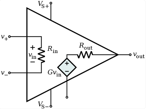
Figure. 1
III. Ideal Operational Amplifier
An ideal operational amplifier should normally have the following characteristics:
1) infinite open-loop gain (Ado = +∞): an important property of the ideal operational amplifier is the open-loop state, the differential signal at the input has an infinite voltage gain, this characteristic makes the operational amplifier in practice is very suitable for applications with negative feedback configuration.
2) Infinite input impedance (Zin / Rin = ∞): the ideal operational amplifier input does not allow any current inflow, that is, in the figure above, V + and V - the two endpoints of the current signal is always zero, that is, the input impedance is infinite.
3) Zero input distortion voltage
4) infinite bandwidth (BW = ∞) and zero phase shift and infinite swing: the ideal operational amplifier for any frequency of the input signal will be the same differential gain amplification, not because of changes in signal frequency and change.
5) Zero output impedance (Zout/Rout = ∞): the output of the ideal operational amplifier is a perfect voltage source, regardless of how the current flowing into the amplifier load changes, the amplifier's output voltage is constant for a certain value, that is, the output impedance is zero.
6) Zero noise
7) Infinite common mode rejection ratio (CMRR = ∞): The ideal operational amplifier can only respond to the difference between the voltage at the two endpoints of V+ and V-, i.e., it only amplifies the part of (V+ - V-). For the same part of the two input signals (i.e. common mode signal) will be completely ignored.
8) Infinitely large supply voltage rejection ratio
All these idealizations cannot be fully realized. Equivalent resistances and capacitances can be used in the op-amp model to simulate the non-infinite or non-zero parameters of a real op-amp. The designer can then take these effects into account in the overall performance of the final circuit. Some parameters may have a negligible effect on the final design, but others that actually govern the final performance must be calculated.
IV. Application of Operational Amplifier
(1) Inverting Closed Loop Amplifier
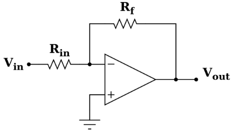
Figure. 2
The above figure shows the circuit of an inverting closed-loop amplifier. Assuming that this closed-loop amplifier uses an ideal operational amplifier, the two inputs of the operational amplifier are falsely grounded because its open-loop gain is infinite. Since the input impedance is infinite, the current from Vin to V- is equal to the current from V- to Vout:
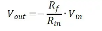
Figure. 3
(2) Positive phase closed loop amplifier
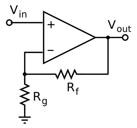
Figure. 4
The above figure shows the circuit of a positive-phase closed-loop amplifier. Negative feedback through the voltage divider resistors Rf, Rg determines the closed loop gain Acl = Vout/Vin. Equilibrium is established when Vout is just enough to make the inverting terminal voltage equal to Vin. Thus the voltage gain of the whole circuit is 1+Rf/Rg. The output voltage equation has:
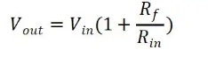
Figure. 5
(3) Adder
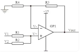
Figure. 6
The above figure shows an adder circuit. Under ideal operational amplifier conditions, since the input impedance is infinite, the currents flowing through R1 and R2 are equal, and similarly the currents flowing through R3 and R4 are equal. Then there is:
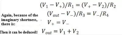
Figure. 7
(4) Integral circuit
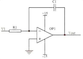
Figure. 8
The above figure shows an integrator circuit. Under ideal operational amplifier conditions, the open-loop gain is infinite, the voltage at the inverting input is equal to that at the coaxial end, and since the input impedance is infinite, the current through R1 is equal to the current through C1.
The output voltage is proportional to the integral of the input voltage over time, and this is the integral circuit.
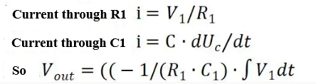
Figure. 9
(5) Differential circuit
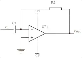
Figure. 10
The above figure shows a differentiator circuit. Under ideal operational amplifier conditions, the open-loop gain is infinite, the voltage at the inverting input is equal to that at the coaxial end, and since the input impedance is infinite, the current through R1 is equal to the current through C1.

Figure. 11
If V1 is a DC voltage added suddenly, the output Vout corresponds to a pulse in the opposite direction to V1.


