

Reversed power supply polarity causing board damage? Here are some solutions.
2025-07-01 11:37:49 1989
Many hardware engineer projects are completed on perforated boards, but there is a risk of accidentally reversing the power supply polarity, which can cause electronic components to burn out and even render the entire board unusable, requiring the board to be rewired. Are there any good solutions to this problem?
Firstly, carelessness is inevitable. Although distinguishing between the positive and negative terminals is as simple as identifying the red and black wires, we might not make a mistake when connecting the wires once, or even ten times. But what about a thousand times? Or ten thousand times? At that point, it becomes uncertain. Due to carelessness, some electronic components and chips may be damaged, primarily because excessive current causes the components to be shorted. Therefore, measures must be taken to prevent reverse connection.
The following are some commonly used methods:
Diode Series Reverse Connection Protection Circuit
A forward-biased diode is connected in series at the positive power supply input terminal, fully utilizing the diode's forward conduction and reverse cutoff characteristics. Under normal conditions, the diode conducts, and the circuit board operates normally.
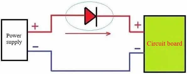
Figure. 1
When the power supply is reversed, the diode blocks the current, preventing the circuit board from functioning, thereby effectively preventing reverse polarity issues.
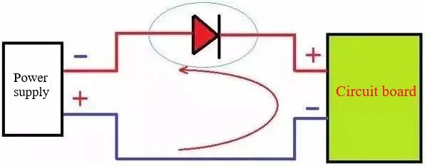
Figure. 2
Rectifier bridge-type reverse polarity protection circuit
A rectifier bridge is used to convert the power supply input into a non-polarized input, ensuring that the circuit board functions normally regardless of whether the power supply is connected correctly or reversed.
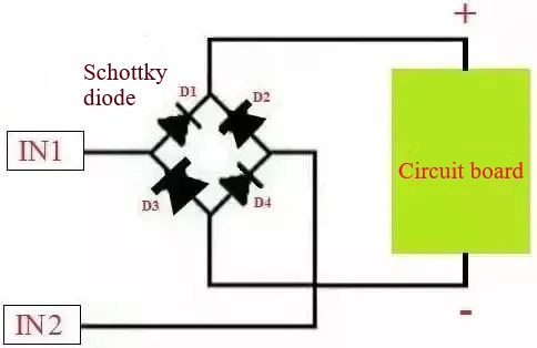
Figure. 3
The above uses a diode for reverse polarity protection. If a silicon diode is used, it has a voltage drop of approximately 0.6–0.8 V, and a germanium diode has a voltage drop of approximately 0.2–0.4 V. If the voltage drop is considered too large, a MOSFET can be used for reverse polarity protection. The voltage drop of a MOSFET is very small, as low as a few milliohms, and can be virtually ignored.
MOSFET Reverse Protection Circuit
Due to advancements in manufacturing processes and inherent properties, MOSFETs have very low on-resistance, often in the milliohm range or even lower. This results in minimal voltage drop and power loss in the circuit, which can be virtually ignored. Therefore, using MOSFETs for circuit protection is a highly recommended approach.
1) NMOS Protection
As shown in the figure below: At power-on, the parasitic diode of the MOSFET conducts, forming a circuit loop. The source (S) potential is approximately 0.6V, while the gate (G) potential is Vbat. The turn-on voltage of the MOSFET is: Ugs = Vbat - Vs. The gate exhibits a high potential, causing the NMOS's drain-source (ds) to conduct, short-circuiting the parasitic diode. The system forms a circuit loop through the NMOS's ds.
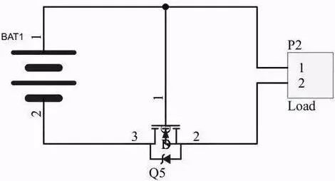
Figure. 4
If the power supply is reversed, the NMOS's turn-on voltage is 0, the NMOS is turned off, the parasitic diode is reverse-connected, and the circuit is open, thereby providing protection.
2) PMOS Protection
As shown in the figure below: At power-on, the parasitic diode of the MOS transistor conducts, forming a loop in the system. The potential at the source (S) is approximately Vbat - 0.6V, while the potential at the gate (G) is 0. The threshold voltage of the MOS transistor is: Ugs = 0 - (Vbat-0.6). The gate exhibits a low level, the PMOS ds conducts, the parasitic diode is short-circuited, and the system forms a loop through the PMOS ds connection.
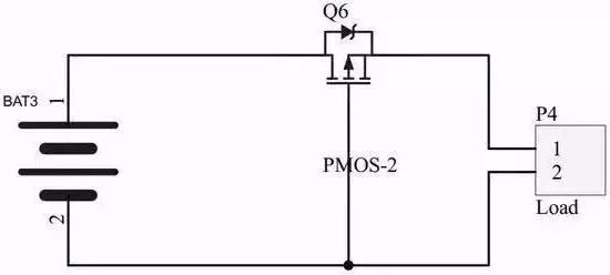
Figure. 5
If the power supply is reversed, the NMOS turn-on voltage is greater than 0, the PMOS is turned off, the parasitic diode is reverse-connected, and the circuit is open, thereby providing protection.
Note: The NMOS transistor connects the ds channel to the negative terminal, and the PMOS transistor connects the ds channel to the positive terminal. The parasitic diode is connected in the correct direction relative to the current flow.
MOS transistor D and S connections: When using an N-channel MOS transistor, current typically flows into the D terminal and out of the S terminal. For PMOS, current flows into the S terminal and out of the D terminal. In this circuit, the direction is reversed, and the parasitic diode conducts to meet the voltage conditions for MOS transistor conduction.
A MOS transistor will fully conduct once a suitable voltage is established between the G and S terminals. Once conductive, the D and S terminals act like a closed switch, with current flowing from D to S or S to D with the same resistance.
In practical applications, a resistor is typically series-connected to the G terminal to prevent the MOSFET from being damaged. A zener diode can also be added for protection. A capacitor paralleled across the voltage-dividing resistor serves a soft-start function. When current begins to flow, the capacitor charges, gradually establishing the voltage at the G terminal.
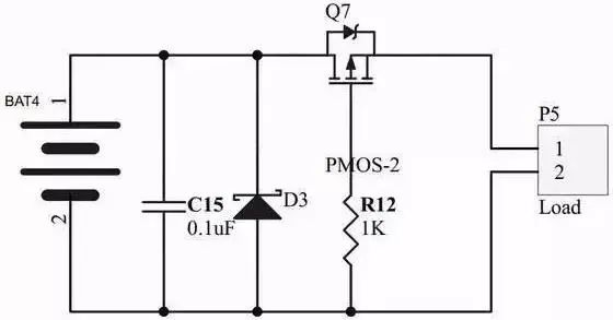
Figure. 6
For PMOS, compared to NMOS, conduction requires Vgs to be greater than the threshold voltage. Since its turn-on voltage can be 0, the voltage difference between D and S is small, giving it an advantage over NMOS.
Fuse Protection
In many common electronic devices, upon disassembly, you can see that the power supply section is equipped with a fuse. When the power supply is reversed or a short circuit occurs in the circuit, the fuse melts due to the high current, thereby protecting the circuit. However, this method is inconvenient for repair and replacement.


