

Implementation of a Micro 3D Endoscope Based on FPGA and OV6946
2025-08-14 14:42:05 1752
1. Introduction
Micro endoscopes typically operate in confined environments with relatively small operating spaces and are widely used in fields such as medicine, aerospace, semiconductors, and security. In some applications, such as minimally invasive surgery and neurosurgery, more precise stereoscopic positioning is often required. However, conventional endoscopes typically use a single lens, which only produces two-dimensional images and cannot provide accurate three-dimensional information.
This solution utilizes a binocular vision system composed of two micro image sensors and an FPGA. The front-end and instrument ends are connected by flexible materials. The system features a small size, flexible operation, high image quality, and is handheld.
2. Overall System Design
2.1. System Introduction
FPGA, short for Field Programmable Gate Array, is a highly configurable integrated circuit that can be programmed using a hardware description language after manufacturing to implement specific functions. FPGAs offer advantages such as parallel processing capabilities, high throughput, and low latency, and are widely used in signal processing, image processing, industrial control, and other fields. The optical lens uses the OV6946 chip, which is a small imaging element launched by OmniVision for the medical market [1]. It is only 0.9 × 0.9 mm in size, and the image resolution can reach 400 × 400@30fps. In addition, the ISP unit is integrated on the chip, which can implement image processing algorithms such as BLC, AEC/AGC and MWB. Even with the integrated LED lighting, the module size can be about 1.2 mm after packaging, which makes it very suitable for endoscope applications. Since the image output by the OV6946 itself is an analog signal, it is generally used in conjunction with the OV426 chip bridge [2] to output the DVP digital signal. This solution integrates two OV6946 chips. The analog image signal output by them is transferred through the OV426 and connected to the FPGA through the DVP interface. The FPGA and the computer are connected through the EZUSB FX3 module [3] to transmit real-time images.
2.2. Technical Features
1) Small size, suitable for occasions with extremely high space requirements.
2) A binocular 3D imaging solution provides enhanced stereoscopic vision.
3) Utilizing FPGA logic triggers to synchronize the two image sensors, frame synchronization within two pixels is achieved. This offers significant advantages in stereoscopic imaging synchronization.
4) No complex binocular video algorithms or lens calibration are required; stereo images can be displayed using a 3D headset in left-right mode.
5) Two hardware configurations support both traditional PC-connected headset display and embedded output directly to a 3D headset.
3. Hardware Implementation
3.1. Mechanical Structure
In terms of hardware, this solution utilizes two OV6946 and OV426 chip sets. The two OV6946 chips and LED lighting form the front-end device, while the back-end circuit board integrates the FPGA and two OV426 chips. Flexible flexible printed circuit boards (FPCs) connect the front and back ends, ensuring device flexibility. The PCB uses an FPGA to capture raw Bayer-format images and integrates an internal ISP processing unit. The processed images are combined into a single left-right image, which is then output to a display via HDMI. This enables 3D imaging when used with a 3D headset. Furthermore, an EZUSB FX3 module is integrated on the PCB, outputting standard UVC-format images. This can be connected to a PC for real-time 3D display using common software such as VLC.
The front end of the device utilizes a dual OV6946 module, with the two modules mounted side by side and surrounded by an integrated LED lighting unit. The output signals from the two modules and the power supply for the LED lighting are simultaneously connected to the back end circuit board via a flexible FPC cable. The FPC length is customizable, supporting lengths of approximately two meters, suitable for common medical procedures.
3.2. Circuit Structure
The two front end lenses are connected to the back end circuit board via a flexible FPC cable. The circuit board integrates the FPGA and two DDR3 x16 chips, forming a 32-bit DRAM. An HDMI chip provides an optional HDMI output for external display connection. An EZUSB FX3 chip can connect USB 3.0 to a PC.
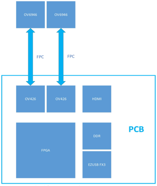
Figure. 1 Overall hardware architecture
3.3. FPGA Selection and Introduction
The FPGA used is the AMD XC7Z020CLG400-2, a programmable system-on-chip (SoC) from the Zynq-7000 series. It integrates an FPGA and a dual-core ARM Cortex-A9 processor, suitable for high-performance applications such as embedded computing, signal processing, and industrial automation. Its main features include:
1) FPGA + ARM Processor: On-chip integration of FPGA logic and the ARM Cortex-A9 makes it suitable for embedded computing and hardware acceleration.
2) High-performance DSP Computing: Built-in 220 DSP computing units, suitable for signal processing, image processing, and AI acceleration.
3) Flexible I/O Design: Supports multiple interfaces (USB, PCIe, UART, SPI, I2C, CAN, and SDIO). 4) Rich storage options: NOR/NAND Flash, SD/eMMC storage.
5) Low-power design: Suitable for embedded and battery-powered systems.
3.4. 3D Headset Display Module
3D headset displays primarily utilize a range of hardware and display technologies to deliver immersive three-dimensional images and interactive experiences. The core principle is binocular parallax 3D imaging. Specifically, 3D helmets typically feature two displays (one for each eye) or a single display, with optical separation technology (such as lenses) allowing each eye to see a different image. This approach mimics the parallax effect of the human eye: each eye sees a slightly different perspective, which the brain synthesizes to create depth perception.
At the same time, when the left and right eyes see slightly different images (based on stereoscopic camera images), the brain combines these images to produce three-dimensional depth perception, resulting in an immersive visual experience.
When selecting a 3D display helmet, simply use a common device that can be connected to a PC via HDMI. The PC streams the displayed image to the helmet in real time, while also outputting a flat image to an external monitor for viewing. After turning on the left and right 3D modes of the 3D helmet, the user can observe a 3D image by placing their eyes close to the helmet.
4. FPGA Implementation Solution
4.1. Overall FPGA Implementation Framework
The FPGA system framework is shown in Figure 2. All modules provide AXI4-Lite slave interfaces, which are mounted on the FPGA's AXI bus. This allows the ZYNQ-7000 chip's ARM processor to read and write internal registers online, thereby modifying each module's configuration.
The overall FPGA design block diagram is shown in Figure 2:
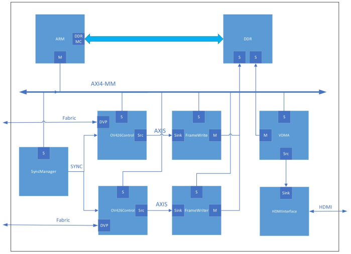
Figure. 2 FPGA block diagram
4.2. OV426 Control Module
Two OV426 modules are implemented within the FPGA, connected to each module via a 10-bit DVP interface to transmit real-time images. The SCCB module within the module is used to initialize and modify CMOS configurations online, such as white balance and window size. System anomalies are reported to the ARM via the INT_o interrupt pin. It should be noted that traditional camera synchronization solutions are generally based on microcontrollers and ASICs. To achieve frame synchronization, they use a "soft" synchronization method handled by upper-level software. This solution, however, cannot guarantee the synchronization of the original image. This solution, based on an FPGA, adds SYNC_i synchronization logic external to each of the two OV426 modules. This unified external synchronization achieves "hard" synchronization of the original image at the hardware level. Experimental results show that this solution can achieve frame synchronization within two pixels.
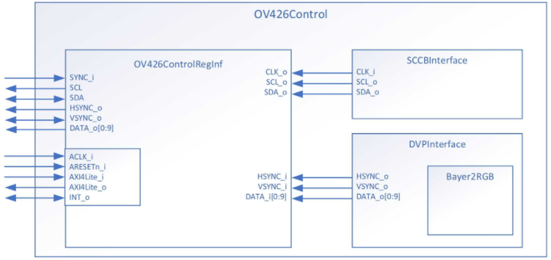
Figure 3. OV426 block diagram
4.3. EZUSB FX3 Control Module
The host computer and FPGA communicate using the EZUSB FX3 module, a flexible USB controller from Infineon Technologies. It offers a theoretical transfer rate of 5 Gbps and measured speeds exceeding 260 Mbps. It can transmit 1080p @ 30 Hz video. For two sets of 400 × 400 @ 30 fps images, the actual bandwidth is fully sufficient.
The EZUSB FX3 module is implemented within the FPGA and connected to the EZUSB FX3 module via a 10-bit parallel port to transmit real-time images. The module also implements a state machine to monitor and manage system states such as data transfer mode, buffer fullness, and data validity.
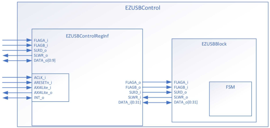
Figure. 4 EZUSB block diagram
5. Software Implementation
5.1. EZUSB FX3 Firmware Implementation
EZ-USB FX3 supports multiple operating modes to meet different application requirements. These modes can be flexibly switched through FX3 configuration to adapt to different hardware and data transfer requirements. Common operating modes include:
1) Host mode. FX3 acts as a USB host to communicate with external USB devices.
2) Peripheral mode. FX3 acts as a USB peripheral to an upstream USB host.
3) Data transfer mode. Support for USB 3.0 mode enables high-bandwidth device applications such as HD video capture and streaming.
4) UVC (USB Video Class) peripheral mode. FX3 acts as a USB video device, transmitting video streams over the USB interface.
5) GPIF (General Programmable Interface) mode. This enables high-bandwidth, low-latency data transmission with peripherals.
6) Synchronous clock mode. This allows precise timing control when exchanging data with other peripherals in sync with the clock.
7) Asynchronous transfer mode. This mode allows data transmission with peripherals and is suitable for most stream-based transfer applications.
In this application, the FX3 firmware is modified to operate in data transfer mode. EZUSB FX3 performs bulk real-time data acquisition, with a single block transfer size of 16 KB.
5.2. Host Driver Implementation
To reduce image display latency and improve the system's real-time performance, image acquisition, processing, and display utilize a multi-threaded asynchronous architecture. Data is buffered in a thread-safe, circular queue, ConcurrentQueue, using a producer-consumer model. The data acquisition thread acts as the producer, placing acquired images into the buffer queue and operating at the highest priority to ensure frame integrity and maximize system reliability. The image processing thread acts as a consumer, reading image frames from the buffer queue and dispatching them to the GUI thread after processing, ensuring a smooth user interface.
The host computer software and FPGA data flow follow a custom frame synchronization protocol to ensure the integrity and validity of each frame.
The host computer software architecture is shown in Figure 5:
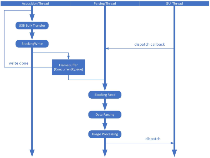
Figure. 5 Software Architecture
5.3. Host Computer Graphical Interface
This application processes the real-time images from the two image sensors and displays them full-screen on the left and right sides of the monitor. The original 400 × 400 image is compressed into two 200 × 400 images, each displayed on the left and right sides.
The actual imaging effect is shown in Figure 6:
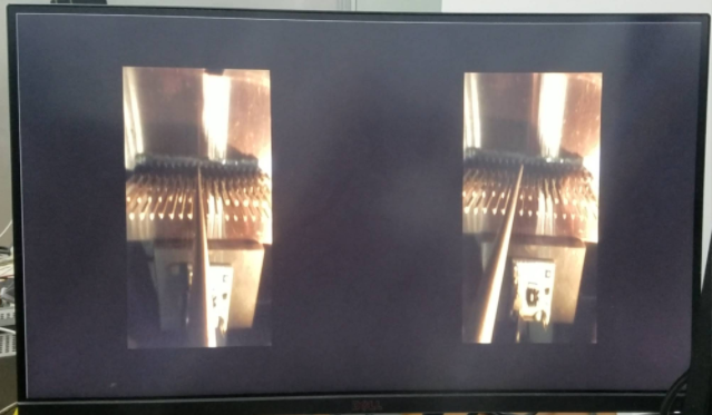
Figure 6. Realtime Image Picture
6. Completion Status
As of the time of publication, all mechanical, software, and hardware work has been completed and has been applied in actual simulation experiments.
Figure 7 shows the real-time imaging system of a 3D endoscope simulating remote instrument operation. The red part in the figure marks the 3D endoscope body and 3D helmet.
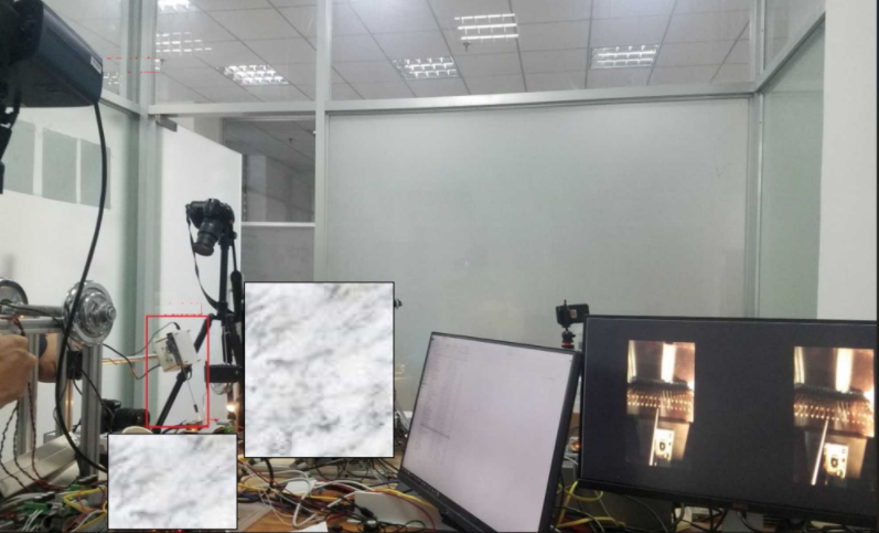
Figure. 7 Finished product picture
7. Future Outlook
In the future, the system optimization of micro 3D endoscope on FPGA will be mainly considered in the following aspects [4]-[6].
7.1. FPGA integrated image processing
1) Stereo matching: FPGA can accelerate the depth calculation based on binocular or multi-eye stereo vision to improve the real-time performance of 3D imaging.
2) Image denoising and enhancement: Image filters can be integrated inside the FPGA to enhance contrast and optimize the endoscopic image quality.
7.2. Data compression
1) Real-time data compression: Use FPGA to accelerate compression algorithms such as JPEG, JPEG2000, H.264/265 to reduce data bandwidth requirements.
2) High-speed interface support: CMOS with interfaces such as MIPI and LVDS can improve the data transmission rate of the endoscope system.
7.3. AI and image analysis
Target detection and segmentation: FPGA-based neural network (such as CNN) acceleration is used for lesion detection, tissue classification, etc.


