

Exploring Power Supplies: From Reverse Polarity to Output Stability
2025-09-28 11:45:20 1673
Reverse Polarity Protection in Power Supplies
When I first encountered this concept, I spent a long time trying to grasp it and found it quite challenging. Let me break it down thoroughly here. There are essentially two key points:
1. Once a MOSFET is turned on, it allows current flow in both forward and reverse directions;
2. The body diode within the MOSFET can carry current. This differs from pure IGBT single transistors.
First, it's essential to know that NMOS and PMOS are different. Reverse polarity protection in power supplies typically uses PMOS. How do you distinguish them? Look at the gate arrow: pointing toward the gate indicates an NMOS, while extending from the gate indicates a PMOS. The following is a reverse polarity protection circuit using a PMOS.
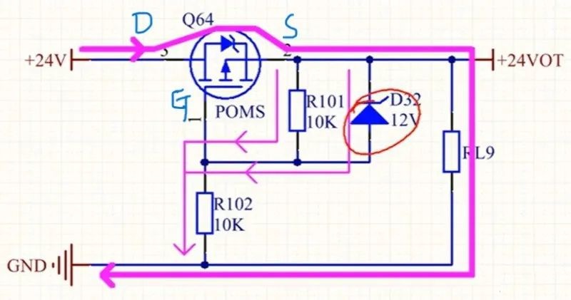
Figure. 1
When the power supply is correctly connected, the body diode conducts with a voltage drop, creating a voltage difference across VGs. This turns on the P-MOS, allowing current to flow from its drain to source. During reverse connection, the body diode turns off, eliminating the Vgs voltage difference. This prevents current from returning to the negative terminal, thus blocking conduction.
MOSFET Conduction
Power drive circuit design is a critical aspect of power supply circuit design, with MOSFETs being the most widely used components. The primary factor affecting MOSFET performance is its input capacitance, specifically the gate-drain capacitance (Cgd), also known as the gate capacitance. This explains why voltage-driven switching devices require a gate drive resistor—the resistor creates the necessary current flow.
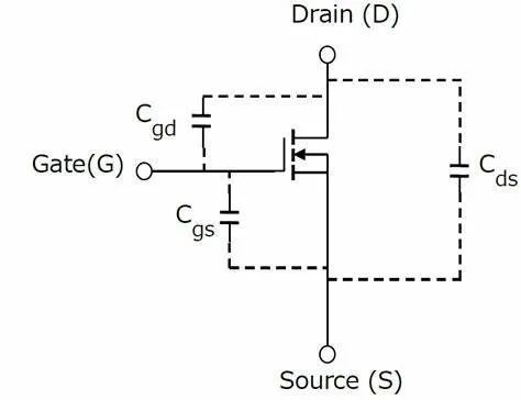
Figure. 2
When the GS voltage rises to the MOSFET's threshold voltage, the IGBT turns on. Current begins flowing through the Ids side, simultaneously causing the Vds voltage to drop (as conduction begins, the internal resistance decreases). During this continued Vds decline, the Vgs voltage slightly decreases to a certain value and remains nearly constant, maintaining a specific voltage plateau—the Miller plateau. This plateau phase is precisely when the Cgd capacitance charges. During this period, the Vds voltage drops completely to 0V, after which the Vgs voltage continues to rise, driving the output voltage of the chip.
Therefore, the methods to reduce the Miller effect can be summarized into two points: reducing Cgd and increasing the threshold voltage.
However, from the perspective of driver circuit design, the following approaches are available:
1. Use negative voltage drive;
2. Employ different resistive paths for turn-on and turn-off, using a smaller Goff resistance;
3. Employ a driver chip with Miller clamping functionality. Miller clamping allows the input capacitor loop to return directly to the negative terminal via the clamping circuit when the MOSFET turns off. This significantly reduces the likelihood of the gate voltage exceeding the threshold voltage during the turn-off transition, thereby minimizing the probability of parasitic conduction.
Switching Power Supply
The most fundamental configurations are the BUCK and boost circuits.
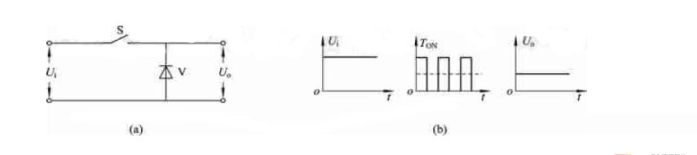
Figure 3
The operating principle of switching power supplies can be illustrated by the diagram above. The unstable DC input voltage Ui is applied to the output via switch S. S is a controlled switch—a switching transistor regulated by switching pulses. By adjusting the conduction or cutoff time of switch S as required, the input DC voltage Ui can be converted into a rectangular pulse voltage. This pulsed voltage undergoes smoothing and filtering through a filter circuit to produce a stable DC output voltage Uo.
Subsequent developments introduced numerous power supply topologies. Many designs, including flyback power supplies, half-bridge drivers, and full-bridge drivers, can be conveniently engineered using software developed by current semiconductor companies. Examples include Infineon's DC/DC design tools, as well as solutions from Toshiba, MPS, and others.
Output Power Supply Stability
This directly tests the design's quality. The most critical aspect is the design of digital and analog grounds. The most common approach is single-point grounding, where digital and analog grounds are connected via ferrite beads or zero-ohm resistors. Bypass capacitors should be placed as close as possible to the chip ports, minimizing the feedback (FB) loop, and output capacitors should be added.


