

EP4CGX15BF14C8N FPGAs: Features, Applications and Datasheet
2025-05-23 11:50:27 1512
EP4CGX15BF14C8N Description
The EP4CGX15BF14C8N is a member of Intel's (formerly Altera) Cyclone IV GX family of FPGAs, optimized for low-power, high-speed serial transceiver applications. Packaged in a compact 324-ball FineLine BGA (FBGA) format, this device integrates transceiver capabilities with mid-range logic resources, making it ideal for high-speed connectivity in cost-sensitive designs.
EP4CGX15BF14C8N Features
Logic Elements (LEs): ~15,408
Embedded Memory: ~540 Kbits
Integrated Transceivers: Supports 2.5 Gbps per channel
Maximum I/O Pins: 148
Operating Voltage: Core: 1.2V; I/O: 1.2V–3.3V
PLL Resources: 2 dedicated PLLs for clock management
Embedded Multipliers: Up to 63 for DSP functions
Low Static Power: Ideal for power-sensitive applications
Package: FBGA-324, compact and thermally efficient
Temperature Range: Commercial (0°C to +85°C)
EP4CGX15BF14C8N Applications
High-Speed Communication Interfaces (e.g., PCIe, Serial RapidIO)
Low-Cost Transceiver-Based Designs
Industrial Automation Controllers
Software Defined Radios (SDRs)
High-Speed Data Acquisition Systems
Digital Signal Processing (DSP) Engines
Medical Imaging and Monitoring Systems
EP4CGX15BF14C8N CAD Model
Symbol
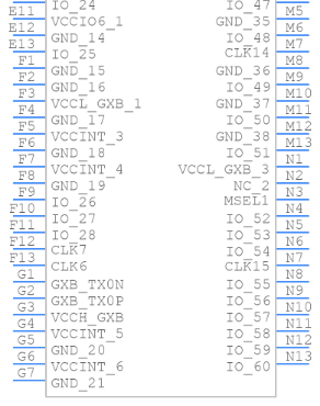
Footprint
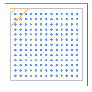
3D Model


EP4CGX15BF14C8N Alternatives
If EP4CGX15BF14C8N is unavailable or over-spec’d, consider these alternatives:
EP4CGX22BF14C8N – Same family with more LEs and memory
EP4CGX15CF23C8N – Larger package variant with same logic density
EP4CE15F17C8N – Cyclone IV E (non-GX), no transceivers
Lattice ECP3-17EA – Similar logic density with embedded SerDes
Xilinx Artix-7 XC7A15T-1CPG236C – Comparable in logic and I/O, with modern toolchain support
EP4CGX15BF14C8N FAQs
Question: What is the practical SERDES latency when interfacing with 2.5 Gbps channels?
Answer: The end-to-end latency (TX+RX) is approximately 10–15 cycles at 2.5 Gbps, depending on the PLL and clock recovery configuration. Proper alignment of clock domains is essential to minimize latency jitter.
Question: What is the power ramp-up sensitivity for the core voltage supply?
Answer: The core 1.2V supply must ramp within 10ms to ensure reliable device initialization. A slower ramp may cause configuration failures or unstable I/O behavior during initial power-up.
Question: Can EP4CGX15BF14C8N tolerate hot-plugging on any of its transceiver lanes?
Answer: Not inherently. The device requires proper ESD protection and power sequencing. Transceiver lanes are sensitive to out-of-sequence power, which may lead to latch-up or permanent damage.
Question: How many independent reference clocks can be fed to the transceiver blocks?
Answer: Two distinct reference clocks can be routed simultaneously—one per transceiver bank. Each transceiver PLL can select from multiple clock sources via dynamic reconfiguration.
Question: Is dynamic reconfiguration of transceivers possible without reloading the entire FPGA?
Answer: Yes. The Cyclone IV GX supports dynamic reconfiguration of transceiver parameters (e.g., equalization, VOD, pre-emphasis) using the ALT_RECONFIG IP without requiring a full reconfiguration.


