

EP1C3T144C8N FPGAs: Features, Applications and Datasheet
2025-11-10 10:40:24 1409
EP1C3T144C8N Description
The EP1C3T144C8N is part of the Altera Cyclone® FPGA family, designed for cost-sensitive applications that still demand high performance, low power consumption, and flexibility. This device is fabricated using advanced CMOS technology and integrates embedded memory, phase-locked loops (PLLs), and a high-speed logic fabric to deliver efficient programmable solutions for embedded systems and digital designs.
EP1C3T144C8N Features
Logic Elements (LEs): 2,910
Embedded Memory: 59,904 bits of on-chip RAM
Embedded Multipliers: 13 × 9-bit multipliers
PLL Support: 1 phase-locked loop for precise clock management
I/O Pins: 104 user I/O pins
Package: 144-pin TQFP (Thin Quad Flat Package)
Core Voltage: 1.5 V nominal
Speed Grade: C8 (moderate-speed performance version)
Configuration: Supports Active Serial, Passive Serial, and JTAG configuration modes
EP1C3T144C8N Applications
Industrial automation and control systems
Communication and networking equipment
Consumer and portable electronics
FPGA-based embedded controllers
Prototyping and digital signal processing systems
Interface bridging and custom peripheral logic
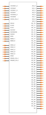
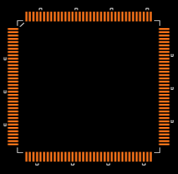
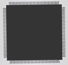
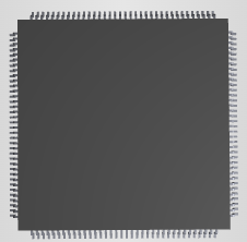
EP1C3T144C8N CAD Model
Symbol
Footprint
3D Model

EP1C3T144C8N Alternatives
EP1C6T144C8N – Higher logic capacity within the same family
EP2C5T144C8N – Cyclone II upgrade with better performance
5CEFA2F17I7N (Cyclone V) – Modern replacement offering lower power and higher density
XC3S200A-4TQG144C (Xilinx Spartan-3A) – Comparable FPGA from Xilinx
Lattice LCMXO2-1200HC-4TG144C – CPLD/FPGA hybrid alternative for control applications
EP1C3T144C8N Manufacturer
Intel Corporation is a world-leading technology company headquartered in Santa Clara, California, USA, widely recognized as a pioneer in the semiconductor industry. Founded in 1968 by Robert Noyce and Gordon Moore, Intel revolutionized computing through the invention of the microprocessor, which became the core of modern computers and countless digital devices.
Intel designs and manufactures a broad range of products including central processing units (CPUs), graphics processors (GPUs), field-programmable gate arrays (FPGAs), system-on-chips (SoCs), and semiconductors for data centers, artificial intelligence (AI), networking, and edge computing.
With decades of innovation, Intel continues to drive progress in areas such as AI acceleration, autonomous systems, high-performance computing, and advanced process technology (e.g., Intel 3, Intel 18A nodes). The company’s mission is to shape the future of computing and enable global technological advancement through intelligent, connected, and sustainable solutions.
EP1C3T144C8N FAQs
What configuration modes are supported by the EP1C3T144C8N?
It supports Active Serial (AS), Passive Serial (PS), and JTAG configuration, allowing flexible design programming and debugging options.
What is the maximum operating frequency of this FPGA?
The device can typically operate up to 200 MHz depending on logic complexity and routing utilization.
Does the EP1C3T144C8N include internal memory blocks?
Yes, it includes M4K embedded memory blocks totaling nearly 60 Kbits, useful for buffering, FIFOs, and small RAM storage.
Can the EP1C3T144C8N interface with 3.3V logic?
Yes. Although the core operates at 1.5V, the I/O banks support voltages from 1.5V to 3.3V, allowing mixed-signal interfacing.
What design tools are compatible with this device?
The FPGA is fully supported by Intel (Altera) Quartus® II software, enabling synthesis, placement, routing, and simulation.


