Circuit Component Design of Switch Mode Power Supply
2025-04-03 17:19:34 1046
Switch Mode Power Supply (SMPS), also known as switching power supply, switching converter, is a high-frequency electrical energy conversion device, a type of power supply. Its function is to convert a standardized voltage into the voltage or current demanded by the user through different forms of architecture. The input of a switching power supply is mostly AC power (such as utility power) or DC power, and the output is mostly equipment that requires DC power, such as personal computers, and the switching power supply converts the voltage and current between the two. Switching power supply products are widely used in industrial automation control, military equipment, scientific research equipment, LED lighting, industrial control equipment, communications equipment, power equipment, instruments, medical equipment, semiconductor refrigeration and heating, air purifiers, electronic refrigerators, liquid crystal displays, LED lamps and lanterns, communication equipment, audio-visual products, security monitoring, LED light strips, computer chassis, digital products and instrumentation and other fields.
I. Switching power supply circuit composition
The main circuit of the switching power supply is composed of input electromagnetic interference filter (EMI), rectifier filter circuit, power conversion circuit, PWM controller circuit, output rectifier filter circuit. Auxiliary circuits include input over-undervoltage protection circuit, output over-undervoltage protection circuit, output overcurrent protection circuit, output short-circuit protection circuit and so on.
The block diagram of the switching power supply circuit is shown below:
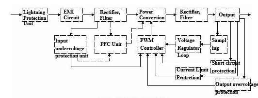
Figure. 1 Switching Power Supply Circuit Block Diagram
II. Principle of input circuit and common circuits
1. Principle of AC input rectifier filter circuit:
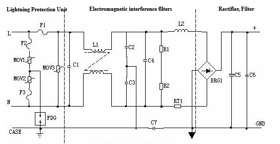
Figure.2 Input Filter and Rectifier Circuit Schematics
① Lightning protection circuit: When there is a lightning strike and a high voltage is introduced into the power supply through the power grid, the circuit composed of MOV1, MOV2, MOV3: F1, F2, F3, FDG1 is protected. When the voltage added to both ends of the varistor exceeds its operating voltage, its resistance value decreases, so that high-voltage energy consumption in the varistor, if the current is too large, F1, F2, F3 will be burned to protect the back stage circuit.
② Input filter circuit: C1, L1, C2, C3 composed of double π-type filter network is mainly for the input power supply electromagnetic noise and clutter signal suppression, to prevent interference with the power supply, but also to prevent the power supply itself from generating high-frequency clutter on the power grid interference. When the power supply is turned on instantly, to charge the C5, due to the instantaneous current is large, add RT1 (thermistor) can effectively prevent the inrush current. Because the instantaneous energy is consumed in the RT1 resistance, after a certain period of time after the temperature rises RT1 resistance decreases (RT1 is a negative temperature coefficient components), then it consumes very little energy, after the circuit can work normally.
③ rectifier filter circuit: AC voltage rectified by BRG1, filtered by C5 to get a more pure DC voltage. If the capacity of C5 becomes small, the output AC ripple will increase.
2. Principle of DC input filter circuit:
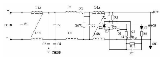
Figure. 3
① Input Filter Circuit: C1, L1, C2 composed of double π-type filter network is mainly for the input power supply electromagnetic noise and clutter signal suppression, to prevent the power supply from interfering with the power supply, but also to prevent the power supply itself from generating high-frequency clutter on the power grid interference. C3, C4 for the safety capacitance, L2, L3 for the differential mode inductors.
② R1, R2, R3, Z1, C6, Q1, Z2, R4, R5, Q2, RT1, C7 form the anti-surge circuit. At the instant of starting, Q2 does not conduct due to the presence of C6, and the current constitutes a circuit through RT1. Q2 conducts when the voltage on C6 is charged to the regulated value of Z1. If C8 leakage or short circuit phenomenon in the back stage circuit, the current in the instant of starting RT1 voltage drop increases, Q1 conduction so that Q2 no gate voltage does not conduct, RT1 will burn in a very short period of time to protect the back stage circuit.
III. The power conversion circuit
1. MOS tube principle of operation: the most widely used insulated gate field effect tube is MOSFET (MOS tube), is the use of semiconductor surface electro-acoustic effect of the work. Also known as surface field effect device. Because its gate is in a non-conducting state, so the input resistance can be greatly improved, up to 105 ohms, MOS tube is the use of the size of the gate source voltage to change the amount of semiconductor surface induced charge, thereby controlling the size of the drain current.
2. Common schematic diagrams:
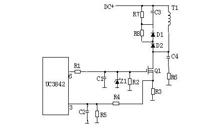
Figure. 4
3. Principle of operation:
R4, C3, R5, R6, C4, D1, D2 form a buffer, and switching MOS tubes are connected in parallel, so that the switching tube voltage stress is reduced, the EMI is reduced, and the secondary breakdown does not occur. In the switching tube Q1 off, the transformer's primary side coil is prone to produce spike voltage and spike current, these components are combined together to absorb the spike voltage and current well. The current peak signal measured from R3 is involved in the duty cycle control of the current operating cycle, and is therefore the current limit of the current operating cycle. When the voltage on R5 reaches 1V, the UC3842 stops working and the switching tube Q1 immediately turns off . R1 and Q1 in the junction capacitance CGS, CGD together to form a RC network, capacitance charging and discharging directly affects the switching speed of the switching tube. r1 is too small, easy to cause oscillation, electromagnetic interference will also be very large; R1 is too large, it will reduce the switching speed of the switching tube. z1 is usually the GS voltage of the MOS tube is limited to 18V or less, thus protecting the MOS tube. The gate controlled voltage of Q1 is a saw wave, when its duty cycle is larger, the longer the Q1 conduction time, the more energy stored in the transformer; when Q1 cutoff, the transformer releases energy through D1, D2, R5, R4, C3, and also achieves the purpose of magnetic reset, which is ready for the transformer's next storage and transfer of energy.IC adjusts the ⑥ according to the output voltage and current at all times. IC adjusts the size of the duty cycle of the saw wave at all times according to the output voltage and current, thus stabilizing the output current and voltage of the whole machine. C4 and R6 are spike voltage absorption circuits.
4. Push-pull power conversion circuit:
Q1 and Q2 will conduct in turn.
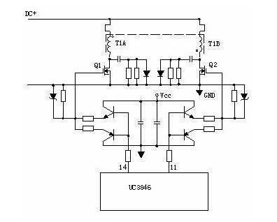
Figure. 5
5. Power conversion circuit with drive transformer:
T2 is the drive transformer, T1 is the switching transformer and TR1 is the current loop.
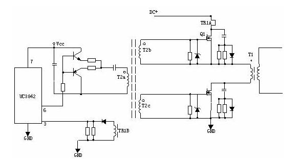
Figure. 6
IV. Output rectifier filter circuit:
1. Forward rectifier circuit:
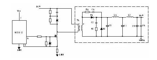
Figure. 7
T1 is a switching transformer, whose primary and secondary phases are in phase. d1 is a rectifier diode, d2 is a continuity diode, r1, c1, r2, c2 is a peak shaving circuit. l1 is a continuity inductor, c4, l2, c5 form a π filter.
2. Flyback rectifier circuit:
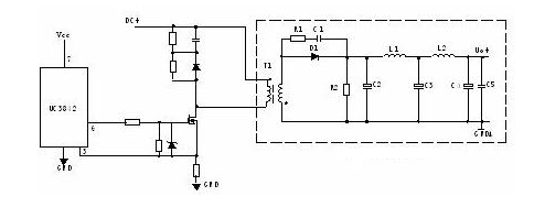
Figure. 8
T1 is a switching transformer with primary and secondary poles in opposite phases, D1 is a rectifier diode, R1 and C1 are peak shaving circuits, L1 is a continuous current inductor, R2 is a dummy load, and C4, L2, and C5 form a π-type filter.
3. Synchronous rectifier circuit:
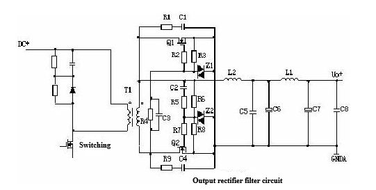
Figure. 9
Principle of operation: when the upper end of the transformer secondary is positive, the current through C2, R5, R6, R7 to make Q2 conduction, the circuit constitutes a loop, Q2 for the rectifier. q1 gate due to the reverse bias and cutoff. When the lower end of the transformer secondary is positive, the current passes through C3, R4, R2 to make Q1 conductive, Q1 is the continuity tube, and Q2 gate is cut off due to reverse bias.L2 is the continuity inductor, C6, L1, C7 form a π-type filter, and R1, C1, R9, C4 are the peak shaving circuits.
Switching power supplies are different from linear power supplies in that they utilize switching transistors that are mostly switched between fully open mode (saturation region) and fully closed mode (cutoff region), both of which are characterized by low dissipation, and the transitions between switches have higher dissipation, but the time is very short, so they are more energy-efficient, and generate less waste heat. Ideally, the switching power supply itself does not consume power. Voltage stabilization is achieved by adjusting the timing of transistor turn-on and turn-off. On the contrary, in a linear power supply, the transistors operate in the amplification region during the generation of the output voltage, which itself consumes power. The high conversion efficiency of a switching power supply is one of its major advantages. Moreover, because of the high operating frequency of a switching power supply, it is possible to use a small-sized and light-weighted transformer, so a switching power supply will also be smaller in size and lighter in weight than a linear power supply. If the high efficiency, size and weight of the power supply are the key considerations, switching power supply is better than linear power supply. However, switching power supply is more complex, the internal transistors will be frequently switched, if the switching current has not been dealt with, may produce noise and electromagnetic interference affecting other equipment, and if the switching power supply does not have a special design, its power supply power factor may not be high.