

ADAS Power Supply Challenges? 75% Capacitor Reduction Solution
2025-08-01 15:52:17 1402
As more and more edge intelligence technologies enter the mainstream, they demand increasingly lower power supply voltage rails to enable real-time local data processing. Applications such as ADAS, infotainment, and body electronics systems in automotive electronics widely adopt edge intelligence technologies. For such applications, the demands on power supply systems are growing increasingly stringent, presenting designers with significant challenges in developing next-generation systems.
To support new market applications and emerging demands, ADI has developed the MAXQ™ Power architecture to maximize performance, significantly reducing performance degradation caused by process and temperature variations in the system's unit gain bandwidth (UGBW), and meeting stringent load transient tolerance requirements. Compared to standard architectures, this architecture can reduce output capacitance by up to 75%, thereby improving load transient performance per µF of output capacitance, which in turn reduces system size, material requirements, and costs.
This article analyzes the core concepts of the MAXQ™ Power architecture, explains how to address critical system design issues, comprehensively analyzes the importance of worst-case scenarios for point-of-load voltage converters, and provides case studies.
The Rise of Smart Edge and Application Demands
For the large-scale application of smart edge, such as the rapid increase in sensor arrays in automotive solutions, these systems previously used one or two cameras but may now require up to 16 cameras, with some autonomous vehicles deploying as many as 96 cameras.
A partitioned architecture using multiple sensors and cameras across various vehicle zones is increasingly favored by automotive manufacturers and OEMs, while the resolution of these sensors and cameras continues to improve. These dense sensor arrays present system designers with multiple challenges, many of which require high-integrity power supplies, local data processing, low latency, and compact sizes.
Traditional solutions are often costly, especially for safety-critical applications, so the urgent need is for cost-effective solutions.
Functions utilizing edge or local processing in vehicle systems include Automatic Emergency Braking (AEB) and Pedestrian Braking, Camera/Radar Fusion, 3D Surround View, Driver Monitoring, In-Vehicle Monitoring, and Electronic Rearview Mirrors. These features were previously common only in high-end vehicles, but with the times, they are becoming increasingly common in consumer vehicles.
The increasing demand for local data processing has led to the use of low-voltage core processor rails within sensor modules. Under high-voltage slew rate heavy-load transients, the processor core rails have very strict voltage tolerance requirements because they power digital processors. This necessitates a high-integrity power supply, meaning that voltage offset should be minimized for given load transients, and reliability must be maintained across a wide temperature range.
Figure 1 shows the load transient response of a high-integrity voltage source for core rail power supply, with minimum and maximum values overlaid. This figure demonstrates that the voltage does not exceed the minimum and maximum tolerances under any load or temperature conditions.
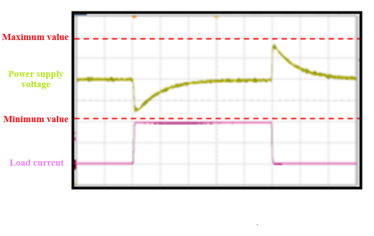
Figure. 1 Example of a high-integrity power supply
When selecting voltage converters for a system, system designers must consider factors such as DC accuracy, load transient response, efficiency, overall solution size, bill of materials, and final solution cost. MAXQ™ Power can address 80% of these requirements.
MAXQ™ Power Buck Converters vs. Standard Buck Converters
What is MAXQ™ Power? Essentially, MAXQ™ Power is a design and testing process aimed at minimizing the impact of IC parameter variations on the voltage converter's unit gain bandwidth, controlling key parameter ratios, while effectively reducing parameter variations across process and temperature ranges.
Benefiting from MAXQ™ Power, the target unit gain bandwidth is significantly improved, enabling the system to operate under more stringent extreme conditions. Compared to standard architectures, MAXQ™ Power converters can maintain performance at lower output capacitance levels.
1. Overview of Unit Gain Bandwidth (UGBW)
Typically, unit gain bandwidth is perceived as a specific point or a specific point under different operating conditions at a specific capacitance or load. However, in reality, there is a probability distribution function, and this probability density function changes with variations in IC parameters and external component parameters. IC control loop parameters change due to internal and external factors, and any deviation from the target in either direction can have a negative impact on the system.
System designers must consider the probability distribution of unit gain bandwidth to ensure their designs perform under worst-case conditions. If the unit gain bandwidth is too high, the system becomes unstable; if it is too low, the loop cannot respond quickly enough, causing voltage shifts.
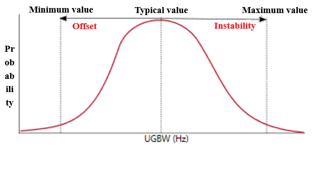
Figure. 2 Unit Gain Bandwidth (UGBW) Distribution
ADI effectively reduces the impact of changes in key parameters affecting the unit gain bandwidth through an iterative design and testing process, and records the relevant data as measurement calculation results. These measurements account for the effects of different temperatures and impose strict limits on the combination of IC factors affecting UGBW using extrapolation methods.
As a result, the probability distribution range of the unit gain bandwidth for any given IC is reduced, enabling the upper limit of available bandwidth to be fully utilized while avoiding the instability issues caused by a wide probability distribution in traditional architectures. Figure 3 illustrates how to effectively narrow the UGBW distribution range and break through the limits.
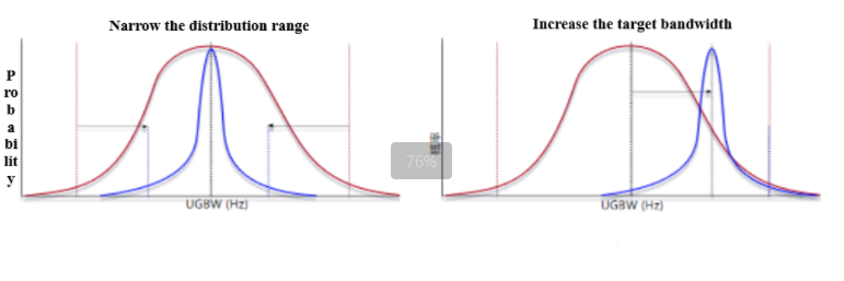
Figure. 3 Example of Effectively Narrowing the UCB7 Distribution Range
2. Time-domain performance of standard buck converters
Using a standard converter with typical unit gain bandwidth as an example, transient response evaluation is conducted under typical operating conditions. The left part of Figure 4 shows the transient response under typical unit gain, assuming the system operates at the lowest COUT under derating. Tolerance is overlaid to display the voltage offset response under a given load transient, with voltage changes maintained within the system's required bandwidth.
The right side of Figure 4 shows another test conducted after modifying the system's unity gain bandwidth distribution based on typical test conditions, adjusting the compensation to keep the fluctuation range of the unity gain bandwidth within 30%. In this case, ripple begins to form, phase margin deteriorates, and the buck converter operates on the edge of instability. The voltage at the lower end of the unity gain bandwidth exceeds the power supply voltage tolerance, which may violate the system's operational requirements and cause a fault.
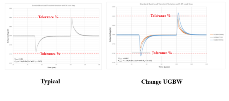
Figure. 4 Example of transient response for a standard buck converter
3. Performance Comparison Between MAXQ™ Power Buck Converters and Standard Buck Converters
Using time-domain transient response as an example, the MAXQ™ Power buck converter is compared with a standard buck converter under identical test conditions: Vout = 0.8V, Iout = 3A, with the unit gain bandwidth pushed to its minimum and maximum values.
In Figure 5, the left side shows that all the curves of the MAXQ™ Power converter are basically overlapping, and the time-domain transient response has almost no deviation, mainly benefiting from MAXQ providing assurance for unit gain bandwidth changes. However, on the right side, the voltage of the standard buck converter exceeds the tolerance at the minimum bandwidth.
The two converters use different capacitor values. The standard architecture uses a 114uF capacitor, while the MAXQ buck converter uses only half the capacitance, i.e., 57uF. Even so, the MAXQ architecture maintains voltage offset tolerance. This is primarily because the MAXQ architecture significantly increases the unit gain bandwidth of the error amplifier to a level far exceeding that of the standard architecture, strictly controlling the extent to which the unit gain bandwidth drifts with IC parameters.
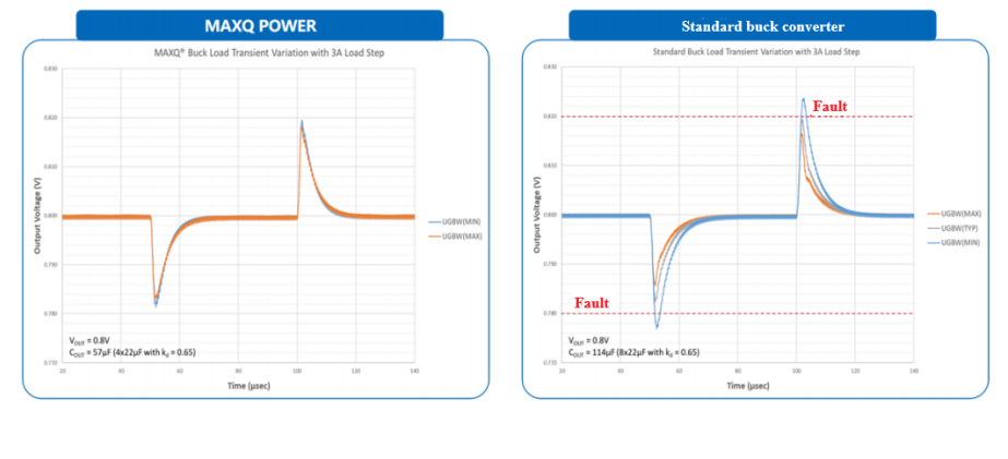
Figure. 5 Impact of gain changes on the transient response of the two converters
From an engineering perspective, the value of the MAXQ™ Power architecture extends far beyond simply reducing capacitance values. As the density of sensors such as cameras and radars in ADAS systems continues to increase, every inch of space and every penny of cost in power design becomes critical—it must withstand instantaneous load surges while maintaining stability in the high-temperature, vibration-prone automotive environment. This “less is more” approach, achieved through precise control of loop characteristics, actually offers design teams a new perspective: instead of piling on components for redundant performance, architectural optimizations can make power systems truly align with the “lightweight and efficient” requirements of edge intelligent devices.
As autonomous driving levels continue to rise, the demands on power systems will only become more stringent. Perhaps in the future, we will see design concepts like MAXQ™ extend beyond capacitor optimization to broader power management domains. After all, in the space-constrained automotive environment, “just the right” performance delivery often holds greater practical significance than blindly pursuing higher parameters. For engineers, understanding the loop design logic behind such architectures may be more effective in addressing the challenges of next-generation electronic systems than simply memorizing capacitor values.


