

PN Junction Diodes as Electronic Switches: Charge Storage Effect & Reverse Recovery Time Impact
2025-06-26 11:01:29 638
PN junction diodes are often used to make electrical switches. In the forward-biased state, i.e., the on state, a small applied voltage can produce a large current; in the reverse-biased state, i.e., the off state, only a small current exists within the PN junction.
The switch circuit parameter we are interested in is the switching speed of the circuit. The following content will qualitatively discuss the switching transient of the diode and the charge storage effect. Without any mathematical derivation, we will simply provide an expression describing the switching time.
The function of a diode
By utilizing the characteristic that the forward and reverse currents of a diode differ significantly, the diode can be used as a switch.
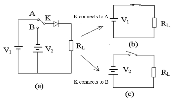
Figure. 1
When switch K is closed to A, the diode is in the forward state, and the current is large, equivalent to the external circuit connected to the load being closed, and the circuit is in the on state (on state);
When switch K is closed to B, the diode is in the reverse state, and the reverse current is very small, equivalent to the external circuit being open, and the circuit is in the off state (off state).
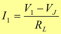
Figure. 2
V1 is the applied power supply voltage, VJ is the forward voltage drop of the diode, approximately 0.7 V for silicon diodes and 0.25 V for germanium diodes, and RL is the load resistance.
In the on state, the steady-state current flowing through the load is I1:
Figure. 3
Typically, VJ is much smaller than V1, so the above equation can be approximated as:
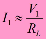
Figure. 4
In the off state, the current flowing through the load is the reverse current IR of the diode.
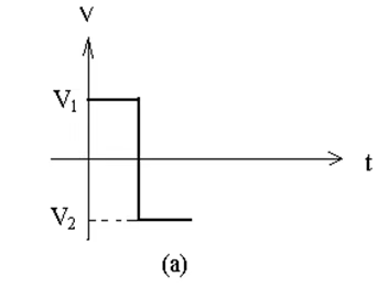
Figure. 5
Assuming the waveform of the applied pulse is as shown in Figure (a), the current flowing through the diode is as shown in Figure (b).
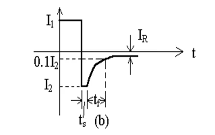
Figure. 6
During the conduction process, the P-region of the diode transports a large number of holes to the N-region, while the N-region transports a large number of electrons to the P-region. As time progresses, the number of holes in the N-region and electrons in the P-region continues to increase until it stops at steady state.
At steady state, the number of holes flowing into the N-region exactly equals the number of holes recombining in the N-region, and the number of electrons flowing into the P-region exactly equals the number of electrons recombining in the P-region, achieving dynamic equilibrium. The current flowing through the P-N junction is a constant I1.
As the hole and electron densities at the boundary of the potential barrier region increase, the voltage across the P-N junction gradually rises, reaching VJ at steady state. At this point, the diode operates in the conducting state.
When a positive pulse applied to the external circuit suddenly changes to a negative pulse:
The large number of minority carriers accumulated in each region during forward conduction are pulled back to their original regions by the reverse bias voltage. Initially, the reverse current flowing through the P-N junction is very large. After some time, part of the originally accumulated carriers recombine, and part are pulled back to their original regions, causing the reverse current to return to the normal reverse leakage current value IR.
The phenomenon of minority carrier accumulation during forward conduction is called the charge storage effect. The reverse recovery process of a diode is caused by charge storage.
The period during which the reverse current remains constant is called the storage time ts. After ts, the current across the P-N junction reaches the reverse saturation current IR, and the P-N junction reaches equilibrium.
The time required for the reverse current flowing through the P-N junction to decrease from I2 to 0.1 I2 is defined as the decay time tf. The sum of the storage time and the fall time (ts + tf) is referred to as the P-N junction's turn-off time (i.e., the reverse recovery time).
The reverse recovery time limits the switching speed of the diode:
If the pulse duration is much longer than the diode's reverse recovery time, the negative pulse can completely turn off the diode, achieving good switching performance;
If the pulse duration is similar to or even shorter than the diode's reverse recovery time, the negative pulse cannot turn off the diode due to the influence of the reverse recovery process.
Therefore, to maintain good switching performance, the pulse duration must not be too short, which means the pulse repetition frequency cannot be too high, thereby limiting the switching speed.


