

PCB Layout Design Points Analysis
2025-05-22 10:23:00 1279
In the electronic circuit system, the printed circuit board (PCB) is to carry electronic components, the realization of the key carrier of the electrical connection, and PCB Layout (Printed Circuit Board Layout and Wiring) design is to determine the performance of the PCB core link. From the signal integrity of electronic products to electromagnetic compatibility, from product reliability to production costs, the quality of PCB Layout design plays a decisive role. The following is a comprehensive analysis of the core elements of PCB Layout design from multiple dimensions.
Layout of special components
Heat-generating components should be placed in a location conducive to heat dissipation, such as the edge of the PCB, and away from the microprocessor chip; special high-frequency components should be placed next to each other to shorten the connecting line between them; sensitive components should be far away from the clock generator, oscillator and other sources of noise; adjustable inductors, variable capacitors, pushbutton switches, potentiometers, and other adjustable components should be in line with the structural requirements of the machine, easy to adjust; heavier components should be fixed with a bracket; the quality of the heavier components should be fixed with a bracket; the PCB Layout design is a very important factor. Heavy components should be fixed with a bracket; EMI filter should be placed close to the EMI source.
Placement of crystal oscillator
The crystal is composed of quartz crystals, easily affected by external impact or fall, so in the layout, it is best not to be placed on the edge of the PCB, as close as possible to the chip placement. The placement of the crystal needs to be far away from the heat source, because the high temperature will also affect the frequency deviation of the crystal.
Device decoupling rules
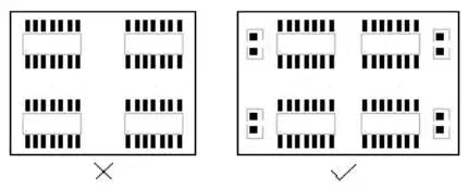
Figure. 1
Add necessary decoupling capacitors on the printed circuit board to filter out the interference signals on the power supply and make the power supply signal stable. It is recommended that the power supply be connected to the power supply pin after passing through the filtering capacitor.
Placement of decoupling capacitors for ICs
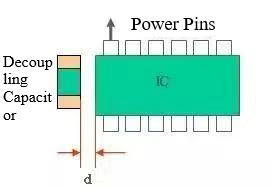
Figure. 2
Decoupling capacitors need to be placed near the power port of each IC, and the position is as close as possible to the power port of the IC, when a chip has more than one power port, decoupling capacitors should be arranged for each port.
Electrolytic capacitors away from heat sources
When designing, PCB engineers should firstly consider whether the ambient temperature of the electrolytic capacitor meets the requirements, and secondly make the capacitor as far away from the heat area as possible, in order to prevent the liquid electrolyte inside the electrolytic capacitor from being baked dry.
Pitch between the chip
Patch components between the spacing is an engineer in the layout must pay attention to a problem, between the patch spacing is neither too large (waste of circuit layout), nor too small, to avoid solder paste printing adhesion and welding repair difficulties.
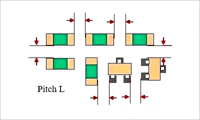
Figure. 3
Pitch size can refer to the following specifications: the same device: ≥ 0.3mm different devices: ≥ 0.13 × h + 0.3mm (h is the maximum height difference between the surrounding neighbors and the device) manual soldering and patching, and the distance between the device requirements: ≥ 1.5mm.
Consistent component lead width
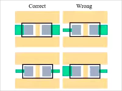
Figure. 4
Retain unused pads
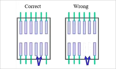
Figure. 5
For example, in the above figure, two of the pins of a chip are not to be used, but the physical chip pins are present, and if the two pins are in a vacant state as in the right side of the above figure, it is easy to cause interference. If the chip pin itself is not connected to the internal, plus the pad and then the pad ground shielding can avoid interference.
The use of over-hole need to be careful
In almost all PCB layouts, it is necessary to use the over-hole in the different layers to provide a conductive connection between the PCB design engineers need to be particularly careful, because the over-hole will produce inductance and capacitance, in some cases, they will also produce reflections, because in the alignment of the production of over-hole, the characteristics of the impedance will change. It is also important to remember that vias increase the length of the alignment and need to be matched. In the case of differential alignments, vias should be avoided wherever possible, and if they cannot be avoided, they should be used in both alignments to compensate for delays in the signal and return paths.


