

GD5F1GM9 QSPI NAND Flash Launches with Breakthrough Read Speed
2025-04-27 11:37:52 1377
Beijing, China, April 15, 2025 - Leading semiconductor device provider GigaDevice (Ticker: 603986) announced the release of the GD5F1GM9 family of high-speed QSPI NAND Flash, which is distinguished by innovative Bad Block The industry's concerns regarding the poor reaction time and susceptibility to bad block interference of traditional SPI NAND Flash may be effectively addressed by the series' innovative Bad Block Management (BBM) feature and breakthrough read speed. The introduction of the GD5F1GM9 series will create new development opportunities for SPI NAND Flash, a new type of solution that skillfully combines the advantages of high-capacity and low-cost NAND Flash with the high-speed read speed of NOR Flash. SPI NAND Flash will be a great option for fast start-up application scenarios like security, industry, and IoT.
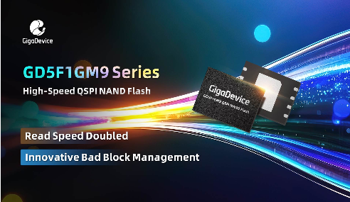
Figure. 1
With a 24nm process node, built-in 8bit ECC, two operating voltages of 3V and 1.8V, and multiple high-speed read modes like Continuous Read, Cache Read, and Auto Load Next Page, the GD5F1GM9 series high-speed QSPI NAND Flash offers users a range of combined design options. The GD5F1GM9 series significantly reduces the calculation time of built-in ECC by doing away with the original serial calculation method in ECC design and implementing parallel computation of sophisticated ECC algorithms. This is in contrast to typical SPI NAND Flash. This line of 3V products has a maximum clock frequency of 166MHz, which allows for a continuous read rate of 83MB/s in Continuous Read mode. The 1.8V products have a maximum clock frequency of 133MHz, which allows for a continuous read rate of 66MB/s in Continuous Read mode. This indicates that the GD5F1GM9 series can achieve read speeds that are two to three times faster than those of conventional SPI NAND products at the same frequency. This design benefit greatly reduces system starting time, further lowers system power consumption, and enhances the device's data access efficiency.
The GD5F1GM9 series adds an enhanced Bad Block Management (BBM) capability to address the bad block issue with conventional NAND Flash. By altering the mapping relationship between physical and logical block addresses, this feature enables users to successfully handle the problems caused by factory bad blocks and newly introduced bad blocks during use. According to one theory, conventional NAND Flashes might have randomly dispersed defective blocks in the factory. If these bad blocks show up in the front code area, the NAND Flash will not function normally. However, the GD5F1GM9 series may assure the stability of the code region by using the Bad Block Management (BBM) function to make sure that the first 256 blocks are all factory good blocks. However, additional faulty blocks could occur while using NAND Flash, and standard methods require a large number of redundant blocks to replace defective blocks in separate partitions, which is a significant resource waste.With the GD5F1GM9 series' BBM feature, users can remap the logical and physical addresses to restore the damaged bad block address and only need to reserve a small number of redundant blocks. This feature not only greatly reduces resource usage but also makes system design much simpler.
According to Ruwei Su, Vice President and General Manager of Mega Innovation's Storage Business Unit, "the GD5F1GM9 series of high-speed QSPI NAND Flash is generally slow at the moment, which has become a significant bottleneck restricting the performance enhancement of end products." The introduction of the high-speed QSPI NAND Flash GD5F1GM9 series has raised the bar for performance in the industry. This series offers a new way to handle faulty blocks, which can be a perfect substitute for NOR Flash users when capacity expansion becomes necessary. It also successfully compensates for the read performance limitations of conventional SPI NAND Flash. To give consumers more dependable and effective storage options, Mega Innovation will also keep refining the underlying technology in the future.
At the moment, the MegaTek GD5F1GM9 series supports WSON8 8x6mm, WSON8 6x5mm, and BGA24 (5x5 ball array) 5x5ball packaging options. It also comes with a 1Gb capacity and 3V/1.8V voltage options. Please get in touch with your local sales representative for further details and prices.
About GigaDevice
One of the top providers of Fabless chips worldwide is GigaDevice (stock code 603986). With its headquarters located in Beijing, China, and branches in numerous nations and regions worldwide, GigaDevice was founded in April 2005 and boasts a global marketing network that offers convenient and high-quality localized support services. Mega Innovation has been certified by the highest level of automotive functional safety ASIL D system of ISO26262:2018, and has also obtained the IEC 61508 functional safety product certification, ISO 9001, ISO 14001, ISO 45001, and other system certification, as well as Dun & Bradstreet certification. Mega Innovation is dedicated to creating a complete ecosystem with memory, microcontrollers, sensors, and analog products as the core driving force. The company also offers complete product technology and services for customers in industrial, automotive, computing, consumer electronics, Internet of Things, mobile applications, and communications. In order to collaboratively advance technological innovation in the semiconductor industry, the company has formed strategic alliances with numerous globally recognized foundries, packaging, and testing facilities.


