

Explained: How to Properly Select Resistors and Capacitors in Bootstrap Circuits
2025-03-21 11:25:01 1725
The industry constantly seeks to reduce the cost of the driver stage in some low-cost applications, particularly for some 600V low-power IGBTs. Because of the circuit's affordability and ease of use, bootstrap power supplies have thus gained popularity as a means of supplying power to high-voltage gate driver (HVIC) circuits.
The Operation of Bootstrap Circuits
Only a 15–18V power source is needed to activate the inverter's driving stage in the bootstrap circuit below. The drivers of the top half-bridge IGBTs are connected to the power supply Vb via resistors Rboot and diodes VF, each of which has a capacitor Cboot to buffer the voltage, whereas all of the bottom half-bridge IGBTs are directly connected to this power source;
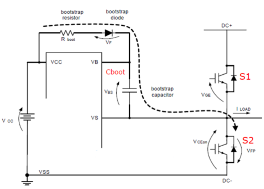
Figure. 1
Vcc charges the bootstrap capacitor Cboot through the bootstrap diode and bootstrap resistor Rboot when the lower tube S2 is turned on to decrease Vs below the supply voltage Vcc. This creates a Vbs suspension voltage across the bootstrap capacitor to facilitate the switching of HO in relation to Vs. When Vs is high voltage and Vbs is disconnected from the power supply Vcc, the bootstrap diode is in reverse bias with the upper tube S1 turned on and off.
Choosing bootstrap capacitors
Every time the lower tube S2 is turned on and the Vs voltage is less than the Vcc supply voltage, the bootstrap capacitor (Cboot) is charged. Only when the high end switch S1 is turned on does the bootstrap capacitor discharge. The high side circuit receives power (VBS) from the bootstrap capacitor. The bootstrap capacitor's maximum voltage drop when the high side switch is on should be taken into account initially. The minimum gate drive voltage that must be maintained determines the maximum voltage drop that can occur (Vbs). The voltage drop across the capacitor must be equal to the VGSMIN minimum gate-source voltage.

Figure. 2
Where:
Vcc = supply voltage of the driver chip;
VF = bootstrap diode forward voltage drop;
Vrboot=voltage drop across the bootstrap resistor;
Vcesat = the on-state voltage drop of the lower tube S2
Calculate the bootstrap capacitance:
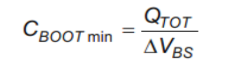
Figure. 3
Where:
QTOT is the total charge of the capacitor.
The total charge of the bootstrap capacitor is calculated by Equation 4:

Figure. 4
The following table calculates the bootstrap capacitance recommendation using the IR2106 + IKP15N65H5 (18A@125°C) as an example:
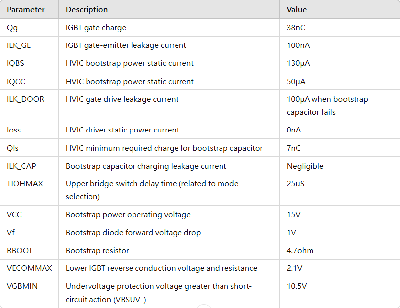
Figure. 5
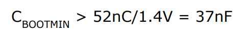
Figure. 6
The device being utilized and the application circumstances must be taken into consideration when choosing the recommended capacitance value. A capacitance value that is too small causes the bootstrap capacitor to drop too much ripple when the upper tube is turned on, which shortens its life, increases switching tube losses, and decreases switching reliability; a capacitance value that is too large shortens the bootstrap capacitor's charging time and may not last long enough to bring the capacitor up to the bootstrap voltage.
Choosing a bootstrap resistor
In order to avoid the bootstrap capacitor from being overly large when it is first charged, the bootstrap resistor's primary role is to control the current. To further illustrate the idea, when an external bootstrap resistor is used, the resistor RBOOT causes an additional voltage drop:
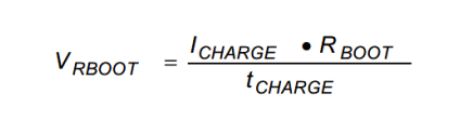
Figure. 7
where:
ICHARGE = charging current of the bootstrap capacitor;
RBOOT = bootstrap resistor;
tCHARGE = bootstrap capacitor charging time (down tube on time)
This resistor's value (usually between 5 and 15 Ω) shouldn't be too high because that will raise the VBS time constant. When determining the maximum permitted voltage drop (VBOOT), the bootstrap diode's voltage drop must be taken into account. We can employ a fast recovery or ultra-quick recovery diode if the circuit does not allow for sufficient charging time or if this voltage drop is excessive.
The real option that we may take into consideration for further bootstrap resistance is too small:
1. Sampling resistor overcurrent protection is triggered when the charging current in small power output applications is very high.
2. A bootstrap resistor that is too tiny may result in increased dVbs/dt, which raises the Vs negative voltage. We shall talk more about the negative voltage's effects later.
3. An excessively high charging current might quickly cause a low VCC voltage during the charging stage, which results in undervoltage protection. 4. Damage from bootstrap diode overcurrent is easily caused.
Design points for bootstrap circuits
You must consider a number of factors to make sure the bootstrap circuit can function correctly:
1. In order to recharge the bootstrap capacitor to the power supply's rated value, the lower bridge arm IGBT of the half bridge should always be conducted first once work begins. Failing to do so could lead to error production and/or uncontrolled switching states.
2. The upper bridge arm driver's energy needs must be satisfied by the bootstrap capacitor Cboot's capacity during the course of an operating cycle.
3. To prevent undervoltage blocking protection, the bootstrap capacitor's voltage must not drop below a certain threshold.
4. There may be a significant peak current when the bootstrap capacitor is first being charged. It is advised to use a low impedance bootstrap resistor to reduce the current because this could disrupt other circuits.
5. Because the bootstrap diode operates at the same frequency as the IGBT, it must be quick, but it also needs to have a blocking voltage that is at least as high as the IGBT's. This implies that a 600V bootstrap diode needs to be chosen for a 600V IGBT.
6. To avoid the IGBT gate voltage being too low and resulting in higher turn-on losses, the internal voltage drop of the driver as well as the voltage drop of the bootstrap diode and bootstrap resistor must be considered when choosing the drive power supply Vcc voltage. Moreover, the calculated voltage needs to be deducted from the lower tube IGBT's saturation voltage drop, which causes the upper and lower tube IGBTs to activate at different positive gate voltages. For this reason, Vcc should make sure the upper tube has an adequate gate voltage while making sure the lower tube gate voltage doesn't rise too high.
7. It is rare to use bootstrap circuits to supply a negative voltage; nonetheless, when doing so, IGBT parasitic conduction must be taken into consideration. It is necessary to address the parasitic conduction of the IGBT. Last but not least, bootstrap circuits have certain drawbacks. For example, in some applications, such as motor drive motors operating for extended periods of time at low speeds and high currents, the lower tube's turn-on duty cycle is relatively small, which means that the upper tube's bootstrap charging is insufficient. In these cases, the PWM algorithm must be used for a particular duty cycle compensation or independent power supply.


