EP2C20F256I8N FPGA: Features, Applications and Datasheet
2024-12-23 11:46:29 1153
EP2C20F256I8N Description
The EP2C20F256I8N is a member of the Altera Cyclone II FPGA family. It is a low-cost, high-performance device designed for applications requiring significant programmable logic, memory, and embedded multipliers. It features a compact form factor with 256-pin FBGA packaging. The device operates efficiently in industrial temperature ranges and is suitable for power-sensitive applications.
EP2C20F256I8N Features
Logic Elements (LEs): 20,060 LEs for versatile design implementation.
Embedded Multipliers: 52 embedded multipliers for DSP applications.
Memory: 239,616 bits of embedded memory.
I/O Pins: Up to 182 user I/O pins.
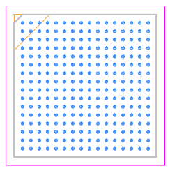
Packaging: 256-ball Fine-Pitch Ball Grid Array (FBGA).
Operating Temperature: Industrial range (-40°C to +100°C).
Power: Optimized for low power consumption.
Speed Grade: Grade 8 (faster performance compared to lower speed grades).
Supported Standards: LVTTL, LVCMOS, PCI, and others.
On-Chip Oscillator: Enables simplified clock generation.
EP2C20F256I8N Applications
Industrial Automation: Real-time control systems and interfaces.
Communications: Baseband processing and protocol translation.
Consumer Electronics: Image and audio signal processing.
Automotive: Advanced driver assistance systems (ADAS).
Medical Devices: Signal acquisition and processing.
Data Acquisition: Test and measurement equipment.
EP2C20F256I8N CAD Model
Symbol

Footprint

3D Model


EP2C20F256I8N Alternatives
EP3C16F256C8N: From Cyclone III family, offering higher density and performance.
EP4CE22F17C8N: Cyclone IV FPGA with more memory and features.
XC3S200A-4FTG256C: Xilinx Spartan-3A series for cost-sensitive applications.
Lattice ICE40HX8K-BG121: Compact, low-power FPGA for mobile designs.
MAX10 Series (10M16DAF484C8G): Integrates flash memory for single-chip solutions.
EP2C20F256I8N Manufacturer
Intel Corporation is a global leader in semiconductor manufacturing and innovation. Founded in 1968 by Gordon Moore and Robert Noyce, Intel pioneered the development of microprocessors, revolutionizing computing technology. Headquartered in Santa Clara, California, Intel designs and manufactures advanced processors, chipsets, and other technologies for personal computers, data centers, artificial intelligence, and the Internet of Things (IoT). Known for its iconic x86 processor architecture, Intel has been instrumental in powering modern computing devices and enabling technological advancements worldwide.
EP2C20F256I8N FAQs
Question: What is the primary advantage of the EP2C20F256I8N?
Answer: The device offers a balance between cost and performance, making it suitable for mid-range industrial and consumer applications.
Question: Can the EP2C20F256I8N support external memory interfaces?
Answer: Yes, it supports interfaces such as SDRAM, SRAM, and Flash.
Question: What development tools are compatible with the EP2C20F256I8N?
Answer: It is compatible with Altera's Quartus II software for design entry, simulation, and synthesis.
Question: Is the device reprogrammable?
Answer: Yes, like all FPGAs, the EP2C20F256I8N is fully reprogrammable, allowing design updates and modifications.
Question: What is the typical use case for its embedded multipliers?
Answer: The embedded multipliers are ideal for digital signal processing tasks such as filtering, FFT, and matrix multiplication.


